The 555timerintegrated circuit (IC) is used in timing, pulse generation, and oscillator applications. It can be configured to generate digital pulses of fixed time lengths. It can also generate continuous pulse trains at given frequencies and duty cycles. In the first case, the 555 timer IC is configured in monostable mode. It creates pulses of defined time lengths determined by a resistor and a capacitor. Each pulse starts when the monostable mode circuit is triggered by a high to low pulse signal. In the second case, the 555 timer IC is configured in astable mode. It creates an oscillator toggling the output between high and low values. A network of resistors and capacitors determines its frequency and duty cycle. In this post we will describe the 555 timer IC. We will also show how to set up the 555 timer IC in monostable and astable modes. The featured image at the beginning of this blog post is from an original published by Swift.Hg – Own work, CC BY-SA 3.0, via Wikimedia Commons.
Inside the 555 IC
The 555 timer IC was designed in 1971 by Hans Camenzind under contract by Signetics. The 555 is probably the most popular timer integrated circuit that was ever designed. It is still in use today, including CMOS versions of the integrated circuit. The schematic on the left, below, depicts the internal block diagram of the 555 IC. The drawing on the right side depicts the pin-out of the 555 timer IC.
There are two symbols in the block diagram that we have not encountered before. Both are made up of a triangle. One or two lines touch the base of the triangle, and a line comes out of the triangle’s summit. In an electronic diagram, triangles represent components called amplifiers. The amplifier inputs are at the base of the triangle. The amplifier outputs are at the triangle’s summit. A small circle means voltage inversion. Voltage inversion can be applied on an amplifier’s inputs or outputs. As the name implies, amplifiers amplify signals. The two triangles at the left with the inverting and non-inverting inputs are called operational amplifiers, or simply, op-amps. The triangle at the right with the inverting output is called an inverter. Both op-amp and inverter components will be discussed in the next paragraph.
Inverters are components used in digital electronics that invert signals. When the input of the inverter is low, its output is high. When the input of the inverter is high, its output is low. Hence, a ‘0’ at the inverter’s input produces a ‘1’ at its output. Similarly, a ‘1’ at the inverter’s input produces a ‘0’ at its output. We do not need to fully describe op-amp operation to explain how the 555 works. Suffices to say that within the integrated circuit, op-amps are used as comparators. Comparators work as follows. When the non-inverting input’s voltage exceeds the inverting input’s voltage, the comparator’s output rises to the supply voltage. This represents a digital high or ‘1’. Otherwise, the output is set to ground. This represents a digital low or ‘0’.
The 555 timer IC block diagram can be broken down in four major stages. The diagram below shows the stages. Stage 1, in the green box, is the voltage divider stage. Three 5 KΩ resistors are connected in series between the integrated circuit’s supply voltage and ground. The voltage divider provides two output voltages to the comparator stage of the 555 timer IC. The first voltage sits at ⅓ the supply voltage, ⅓VCC. The second voltage sits at ⅔ the supply voltage, ⅔VCC. Stage 2, in the yellow box, is the comparator stage. It compares the voltages at the threshold and trigger pins of the NE555 with the voltages of the voltage divider. When the threshold pin’s voltage is larger than ⅔VCC, the flip-flop of stage 3 is reset. When the trigger pin’s voltage is lower than ⅓VCC, the flip-flop of stage 3 is set.
Stage 3, in the blue box, is the state stage. It uses a flip-flop to store the state of the NE555 integrated circuit timer. The inverted output of the flip-flop is low, ‘0’, when a timing cycle has been triggered. The inverted output of the flip-flop is high, ‘1’, when the threshold voltage has been reached. In this state, the timing cycle has completed. The flip-flop can be reset to the timing cycle completed state. The inverted output of the flip-flop drives the output stage. Stage 4, in the red box, is the output stage. The 555 output pin, is high, ‘1’, when a timing cycle is started. The output pin is low, ‘0’, when a timing cycle has completed. The discharge pin is connected to ground when a timing cycle has completed. The discharge pin is floating, as if unconnected, during a timing cycle. The 555 timer IC supply voltage can range between 4.5V and 16V.
Creating a Single Pulse Timer with the 555
A single pulse timer is a timer circuit that activates for a preset amount of time. A 555 timer IC in monostable mode acts as a single pulse timer. To set up the 555 in a monostable mode we need a resistor and capacitor in series. We first put the 555 in the timing cycle state. A capacitor charges through a resistor until the threshold voltage is reached. The 555 then enters the timing cycle completed state and discharges the capacitor. The electronic schematic below illustrates how to build a circuit with the 555 timer IC in monostable mode. The circuit lights an LED for approximately 5 seconds when a push button switch is depressed.
In the circuit above the 555 timer IC is configured in monostable mode. Resistor R and capacitor C form the timing circuit. Resistor R is connected to the supply on one side and to capacitor C on the other. The other end of capacitor C is connected to ground. The resistor-capacitor junction is connected to the 555 threshold and discharge pins. The output pin of the 555 is connected to an LED wit a current limiting resistor. The control pin of the 555 is connected to ground through a 10 nF capacitor. This capacitor is used to prevent external electrical noise from affecting the timing circuitry. The reset and VCC pins of the 555 are connected to the supply. The ground pin of the 555 is connected to ground. Finally, a switch connected to ground is connected to the trigger pin of the 555. The trigger pin is pulled up to the supply voltage by a 10 KΩ resistor connected to the supply. This ensures the the circuit is triggered only when the switch is depressed.
When powered up, the circuit is in timing cycle completed mode. The output is low, the LED is off, and the discharge pin connects the timing capacitor to ground. When the switch is depressed, it grounds the trigger pin. The 555 then enters a timing cycle because the trigger pin is less than ⅓VCC. The output pin becomes high, turning the LED on. The discharge pin becomes floating, allowing the capacitor to charge through the timing resistor. The capacitor charges until its voltage reaches ⅔VCC. As the threshold pin voltage reaches ⅔VCC, the 555 ends its timing cycle. The output pin becomes low and the discharge pin gets connected to ground. The LED turns off and the timing capacitor is discharged. The circuit is then ready for a new timing cycle.
The time it takes for the capacitor to charge depends on the value of the timing capacitor and resistor. In the Switch Debouncing post, we have seen that the voltage across the capacitor of a charging RC (resistor-capacitor) circuit is given by:
VC = VCC (1 − e-t/RC)
The 555 circuit starts in timing cycle mode with the capacitor fully discharged. It remains in this mode until the voltage across the capacitor reaches ⅔VCC. If we want a timing circuit to turn on the LED for t seconds, the equation becomes:
⅔VCC = VCC (1 − e-t/RC)
Solving for t, we get
t = -ln⅓ RC
or approximately
t = 1.1 RC
Note that timing is independent from the supply voltage. Let’s build a circuit that will light an LED for 5 seconds. The RC value that we want is 5 seconds divided by 1.1 yielding 4.55 seconds. If we use a 100 KΩ resistor, we need a 45.5 µF capacitor. A 47 µF capacitor is the nearest standard value. Using a 1 MΩ resistor with a 4.7 µF capacitor would work as well. Any combination of resistor and capacitor values that give 4.55 seconds when multiplied would work. The schematic below depicts a circuit featuring the 555 that turns an LED on for 5 seconds.
The next picture depicts how to connect the different parts using a solderless breadboard and jumper wires. The switch section uses a temporary contact button switch and a 10 KΩ resistor. The RC timing circuit uses a 47 µF electrolytic capacitor and a 100 KΩ resistors. The negative side of the capacitor is connected to ground. The output section uses an LED and a 330 Ω resistor. The anode of the LED is connected to the 555 pin 3. Finally, the board uses a 555 timer IC and a 10 nF ceramic capacitor. Connect the ground, black wires, and supply, red wires, to a suitable power source providing between 5V to 15V.
The LED will turn on for 5 seconds when the button switch is depressed. The 5 seconds start when the switch is first depressed, regardless of how long the button switch is depressed. If the button switch is depressed for more than 5 seconds, the LED will stay lit. It will stay lit until the button is released.
An Oscillator with the 555 Timer IC
In astable mode, the 555 timer IC becomes an oscillator that continuously toggles its output high and low. To set the 555 in astable mode, we need to find a way to re-trigger it automatically. One way to do this is to connect the trigger pin to the timing capacitor. At the end of a timing cycle, the discharge pin discharges the capacitor. The voltage across the capacitor drops below ⅓VCC and the timing cycle starts again. The next schematic shows this configuration.
Although this circuit works, the capacitor discharge time is so short that the LED appears on all the time. One way to slow down the capacitor discharge is to discharge the capacitor through a resistor. The next schematic shows how to do this.
In this new circuit, the timing capacitor is charged through resistors RC and RCD. While the capacitor is charging, the output is high and the LED is lit. When the voltage across the timing capacitor reaches ⅔VCC the threshold voltage is reached and the timing cycle ends. The output goes low, the LED turns off and the capacitor starts discharging through resistor RCD. When the voltage across the timing capacitor drops to ⅓VCC, the timing cycle starts again. While discussing the 555 astable operation we found the time it takes for a capacitor to charge to ⅔VCC. The time it takes a capacitor to charge from ⅓VCC to ⅔VCC through a resistor is
t = (-ln⅓) RC − (-ln⅔) RC
Simplifying the equation we get
t = (-ln½) RC
The equation for the voltage across a capacitor through time as it discharges is
VC = V0e-t/RC
To calculate the time it takes for a capacitor to discharge from ⅔VCC to ⅓VCC, we substitute ⅓VCC for VC and ⅔VCC for V0 in the equation
⅓VCC = ⅔VCCe-t/RC
Solving for t, we get
t = (-ln½) RC
Unsurprisingly, charging a capacitor through a resistor takes the same time as discharging it through the same resistor. The time it takes to charge or discharge a capacitor through a resistor between ⅓VCC and ⅔VCC is approximately
t = 0.69 RC
Hence, the time it takes to charge the timing capacitor C through resistors RC and RCD then discharge through RCD is
t = 0.69 (RC + RCD) C + 0.69 RCD C
or
t = 0.69 (RC +2 RCD) C
Let’s say that we want to create an oscillator flashing an LED at a frequency of 0.2 Hz. We also want the LED to be on 60% of the time. The full cycle time is thus 5 seconds. The LED is on for 3 seconds and off for 2 seconds. The first circuit used a 47 µF capacitor for an on time of 5 seconds. Let’s use a 22 µF capacitor for the new circuit for an on time of 3 seconds. We thus have to find a solution to the two equations
0.69 (RC + 2RCD) 22×10-6 = 5 s — Full cycle time
0.69 (RC + RCD) 22×10-6 = 3 s — Time to charge
Solving for RC and RCD we get RC = 66 KΩ and RCD = 132 KΩ. The closest standard 10% resistor values are RC = 68 KΩ and RCD = 120 KΩ. These values yield a frequency of 0.21 Hz and an LED on time of 2.9 seconds, quite close to the required values. Here is a circuit with a 555 timer IC oscillator. It continuously turns an LED on for 3 seconds and off for 2 seconds.
The next picture depicts how to connect the different parts using a solderless breadboard and jumper wires. .The RC timing circuit uses a 22 µF electrolytic capacitor a 68 KΩ resistor and a 120 KΩ resistor. The negative side of the capacitor is connected to ground. The output section uses an LED and a 330 Ω resistor. The anode of the LED is connected to the 555 pin 3. Finally, the board uses a 555 timer IC and a 10 nF ceramic capacitor. Connect the ground, black wires, and supply, red wires, to a suitable power source providing 5V to 15V.
As soon as the circuit is connected to power, the LED will turn on. It will then turn off for 2 seconds then on again for 3 seconds. The first time it is on, the LED remains lit for over 3 seconds. This happens as it starts charging from 0 volt instead of ⅓VCC.
What Next
We have seen how the 555 timer IC can be used as a delay and as an oscillator. You can start playing with the timing resistor and capacitor values to change the delay, frequency and duty cycle. Notice that in astable mode, the circuit shown can’t provide a 50% duty cycle. The time on is always greater than the time off. This is because of the resistor configuration. Try to find a solution to this limitation. The 555 timer IC can also be used in other applications. It can serve as a memory bit. It can act as a Schmitt trigger. It can function as a voltage-controlled oscillator. Additionally, it can be used as a pulse width modulator, among other uses.
The Arduino Uno is limited to fourteen digital input/output pins and six analog input pins. The analog input pins can also be used for digital input/output thus providing a total of 20 digital input/output pins. In the four digit seven-segment display developed in blog post Driving Seven Segment Displays, twelve digital input/output pins were used, seriously limiting the amount of input/output real estate left. This would be especially true if we were to increase the number of displayed digits and if we needed to do any useful interaction with the environment through sensors. What if we needed tens or even hundreds of digital outputs from a single Arduino Uno? It can be done using digital electronicintegrated circuits called shift registers along with a technique called serial communication.
I have used serial communication throughout my blog posts. We have used it to send and receive Morse code in the Morse Code Reader and Morse Code Generator posts. We have also used it to communicate with the temperature and humidity sensor DHT22 in the Sensing Temperature and Humidity post. In this post, we will use the SN74HC595 8-bit shift registers with 3-State output registers integrated circuits to convert serial signals into a collection digital output values. Using only three of the Arduino Uno’s digital I/O ports we will send digital values to the shift register integrated circuits and we will use the shift register outputs to drive a ten-LED bar graph.
Registers
In digital electronics, a register is a collection of devices, also known as flip-flops, each capable of holding a single bit of information. Effectively, a flip-flop is a single bit of memory. The following diagram depicts a D flip-flop, a device capable of remembering the value of a digital signal, D, when another signal, CLK, goes from a low to a high value, from 0 to 1. The device has two outputs, Q and Q, that provide the device’s remembered value and its inverse respectively. The device has two other inputs, PRE and CLR. The PRE input sets the flip-flop value to a high value, 1, when a low pulse is applied to the input. The CLR input resets the flip-flop value to a low value, 0, when a low pulse is applied to the input.
The previous diagram follows the IEEE Standard 91-1984 which defines how to represent digital electronic components. The device is represented by a box. All input lines are drawn at the left of the box while all outputs are drawn at the right. Lines connected directly to the device represent signals that are active when the value of the signal is high, 1. Lines connected to a small circle attached to the device represent signals that are active when the signal is low, 0. Lines connected to the device through a small triangle represent signals that are active when the value switches from low to high, 0 to 1.
A register, as depicted in the following drawing, is made of several flip-flops, one for each bit of information to be stored. Data is presented at the D input of each flip-flop and the state of each flip-flop is set when the clock signal, attached to the clock input of each flip-flop, is toggled from a low to a high value, 0 to 1. The data stored in the register in the form of bits of information is made available at the output of the flip-flops making up the register. In the diagram, four flip-flops store four bits of information depicted from right to left, least significant bit at the rightmost position and most significant bit at the leftmost position.
Serial to Parallel Shift Registers
a serial to parallel shift register is a register that converts a serial train of bits into a parallel representation. The diagram below depicts the connectivity required to transform a register into a serial to parallel shift register. There are two inputs to the circuit: the data and clock signals. The data signal is connected to the most significant flip-flop’s data input; each flip-flop output is connected to the next less significant flip-flop data input; and the clock signal is connected to every flip-flop clock inputs. At each clock toggle from low to high, flip-flops take the value or the previous more significant flip-flop and the most significant flip-flop takes the value of the data signal. All flip-flop outputs form the parallel representation of the successive serial values of the data signal. By presenting values, a bit at a time, least significant bit first, on the data signal, clocking in each new value, we can convert the serial data signal to a parallel representation of the signal.
The values stored in each flip-flop of the serial to parallel shift register becomes the representation of the serial signal in the end. However, while the bits are being shifted, the flip-flop outputs will contain intermediate values until we finish clocking in all the values. A way to solve this problem is to put a register to store the output of the serial to parallel shift register after all bits have been shifted.
Latched Shift Registers
The following diagram depicts a digital circuit comprised of two registers, a serial to parallel shift register at the bottom and a latch register at the top. As described in the above paragraphs, the serial to parallel shift register converts the serial data signal into its parallel representation by clocking in each bit in turn; when the shifting is done, we can store the values at the output of each serial to parallel shift register flip-flop in the latch register by toggling the latch signal from a low to high value.
The above diagram represents a four-bit latched shift register. The circuit can be extended by repeating each serial to parallel and latch register stages to the right of the circuit by connecting the clock signal to the serial to parallel flip-flop’s clock; connecting the output of the previous less significant flip-flop, called “Next Data” in the diagram, to the data input of the new serial to parallel flip-flop; by connecting the output of the new serial to parallel flip-flop to the data input of the new latch register flip-flop data input; and finally by connecting the latch signal to the clock input of the new latch register flip-flop.
The number of bits that can be supported is almost infinite, only limited by the electrical characteristics of the digital integrated circuits used to implement the circuit and the amount of time required to shift each bit in position. The integrated circuit that will be used to demonstrate how to increase the output capacity of the Arduino Uno is the SN74HC595N 8-bit shift registers with 3-State output registers digital integrated circuit. Internally, the integrated circuit is similar to the digital circuit shown above but has eight bits instead of four. Moreover, the outputs can be put in a high-impedance (high resistance) state, making it behave as if it was not connected. This latter functionality will not be used in this demonstration.
The SN74HC595 Shift Register with Latch
The diagram below is a depiction of the SN74HC595 digital integrated circuit. It describes the integrated circuit functionality on the left, and its pinout on the right. The SN74HC595 integrated circuit is housed in a 16 pin dual in-line package (DIP). The integrated circuit’s pins 8 and 16, not shown on the functional diagram, are used to power the integrated circuit. Pin 8, GND, is to be connected to ground while pin 16, VCC, is to be connected to power, 5 volts. In all of the following text, a LOW value or 0 is represented by a signal at the same potential as the ground, 0 volt, and a HIGH value or 1 is represented by a signal at the same potential as VCC, 5 volts.
The functionality diagram follows the IEEE Standard 91-1984. The two top blocks notched at the bottom represent the integrated circuit’s common control elements. The bottom blocks represent each of the eight serial register flip-flops and the output register flip-flops feeding each other in two stages, from left two right. The topmost serial register is fed external data from the serial data line through the pin labelled SER. The bottommost serial register flip-flop output is directly attached to pin QH‘ which can be used to feed another serial register’s input, allowing the extension of the shift register to many more stages. Each output register flip-flop is attached to pins QA through QH giving access to each of the flip-flop’s value.
There are two common control elements, one for the collection of serial register flip-flops and the other for the collection of output register flip-flops. The first, smaller, common control element has two inputs. The SRCLR input pin is used to reset to a LOW value, 0, all shift register flip-flops when its value is set to LOW for a minimum of 20 ns. The SRCK input pin is the shift register flip-flops’ common clock that shifts in the value of the SER pin and shifts the shift register flip-flop values when the pin is toggled from a LOW to HIGH value, from 0 to 1. The second common control element also has two inputs. The G input pin is used to enable the integrated circuit’s output register flip-flops’ output when its value is LOW or 0 and to leave the output pins in a high impedance state when HIGH or 1. The RCK input pin is the output register flip-flops’ common clock that latches the shift register flip-flop values into the output register flip-flops when the pin is toggled from a LOW to HIGH value.
In order to use the integrated circuit properly, we must understand its most important electrical and timing characteristics. All inputs draw a maximum of 1 μA each. The integrated circuit’s output register’s outputs, QA to QH can source or sink 6 mA. The SRCK and RCK shift register and output register clocks must remain HIGH for at least 20 ns and LOW for at least 20 ns, allowing for a maximum clock frequency of 25 MHz. The SRCLR input pin must remain LOW for at least 20 ns for the serial register flip-flops to be reset. The SER, serial data input, pin must be stable at least 25 ns before the SRCK pin can be toggled from LOW to HIGH to latch the input value.
From the integrated circuit’s characteristics, we can say that an Arduino Uno digital output, which can source or sink 20 mA, can theoretically drive the inputs of up to 20 000 SN74HC595 integrated circuits if we ignore other electrical constraints. There is more to consider than the current required to drive clock inputs. We have to take into account wire lengths, the current required to drive integrated circuit outputs and integrated circuit layout. I would recommend not to daisy chain, that is serially connect clock inputs one after another, more than twenty integrated circuits without carefully considering the design of integrated circuit placement and wiring layout. As for the timing characteristics, the maximum speed at which we can toggle digital outputs on the Arduino, measured with an oscilloscope while executing two digitalWrite() calls is 3.5 μs, which is well above the minimum time of 20 ns required by the SN74HC595 clock inputs.
Creating 10 Digital Outputs from 3 Digital Outputs
We will use two SN74HC595 digital integrated circuits to drive a ten LED bar graph display from three Arduino digital outputs. In the following paragraphs we will discuss the circuit used to control the bar graph display using an Arduino C++ program. The program can be found on GitHub here.
The Electronics
The following diagram depicts the digital circuit we will use to demonstrate how to drive ten bar graph LEDs from three Arduino digital outputs. In the diagram, Arduino’s digital port 3 is connected to both SN74HC595 integrated circuits’ serial clocks, pin 11 of each integrated circuit. Arduino’s digital port 4 is connected to both SN74HC595 integrated circuits’ register latch clocks, pin 12 of each integrated circuit. Arduino’s digital port 2 is connected to serial data input, pin 14, of the SN74HC595 integrated circuit that is to drive the eight most significant, leftmost, LEDs of the bar graph. The serial output of that integrated circuit, pin 9, is connected to the serial data input, pin 14, of the SN74HC595 integrated circuit that is to drive the two least significant, rightmost, LEDs of the bar graph.
As shown on the diagram, the eight outputs of the topmost SN74HC595 integrated circuit are connected to the eight most significant LEDs’ anode of the bar graph through 1K resistors. The two most significant outputs of the bottom SN74HC595 integrated circuit are connected to the two least significant LEDs’ anode of the bar graph display through 1K resistors. All bar graph display LEDs’ cathodes are connected to ground.
The reset pins, pin 10, of each SN74HC595 integrated circuit are connected directly to 5V, preventing the serial shift registers from resetting. The enable pins, pin 13, of each SN74HC595 integrated circuit are connected to ground thus always enabling each latched register’s output. The following timing diagram shows the digital values applied to the shift registers with latch through the Arduino digital ports to output ten digital values to be displayed on the ten LED bar graph display. The top signal in the diagram represents the serial data output by the Arduino at digital port 2. Since the data can be either a 1 or 0, a HIGH or a LOW, we show both with a crossover at the point the value is set. The second line represents the serial register clock output by the Arduino at digital port 3. The third line represents the latched output clock output by the Arduino at digital port 4.
In order to send ten binary values to the bar graph LEDs, an Arduino program must send ten bits, least significant bit first. So, the program sets the value of the least significant bit at digital port 2. The program then toggles the serial clock signal at digital port 3 from LOW to HIGH, then HIGH to LOW. These two steps are repeated for each bit of information until the most significant bit is processed. Finally, the program toggles the latch clock signal at digital port 4 so that all values that were sent serially are provided to all LEDs in the bar graph at once.
Breadboarding the Circuit
The following picture depicts how to connect the different parts using a solderless breadboard, jumper wires, SN74HC595 digital integrated circuits, 1 KΩ resistors, LEDs. and an Arduino Uno micro-controller. In the schematic, I used discrete LEDs instead of a 10 LED bar graph, but the wiring would be identical.
The Program
The program used to demonstrate the use of the latched shift register is made up of the Arduino sketch, UsingShiftRegistersToIncreaseDigitalOutputs.ino, containing the setup() and loop() functions. There is also a class, LatchedShiftRegisterChannel, that embodies the functionality of the serially connected latched shift registers. The class is defined in the LatchedShiftRegisterChannel.h header file and the class methods are implemented in LatchedShiftRegisterChannel.cpp. We described classes in a previous post, Programming with Class. In the next paragraphs we will see how the LatchedShiftRegisterChannel class is implemented and how the main program uses this class to output values to ten LEDs using three digital output ports.
LatchedShiftRegisterChannel.h
The LatchedShiftRegisterChannel.h header file defines the LatchedShiftRegisterChannel class. In the header file, before the class definition, we declare a constant for the maximum number of digital outputs that are supported by the class, MAXIMUM_SERIAL_BITS. We then declare a structure, SerialCommunicationPins, to store the Arduino output ports associated with the serial clock, data, and latch clock pins that are used to drive the shift register integrated circuits. Follows the LatchedShiftRegisterChannel class declaration. There are four public methods. ~LatchedShiftRegisterChannel() is the class destructor called when an instance of the class goes out of scope or gets deleted. The LatchedShiftRegisterChannel()constructor with two arguments is the only constructor supported. It takes a SerialCommunicationPins structure as input as well as the maximum number bits, or digital output ports, that can be driven by the shift registers in the circuit. Each SN74HC595 integrated circuits can drive 8 bits each, hence two shift register integrated circuits can drive 16 bits. The transmit() method is used to output bits to the digital output ports driven by the shift registers. Finally, the setNumberOfActiveDigitalOutputs() method sets the actual number of digital outputs to drive. It is used if the value is different than the number of shift register bits that was set in the constructor.
#if !defined(LATCHEDSHIFTREGISTERCHANNEL_HEADER)
#define LATCHEDSHIFTREGISTERCHANNEL_HEADER
#include "Arduino.h"

const int MAXIMUM_SERIAL_BITS = 1024;

struct SerialCommunicationPins {
  int serialClockPin;
  int serialDataPin;
  int latchClockPin;
};

class LatchedShiftRegisterChannel {
  public:
    ~LatchedShiftRegisterChannel(); // Destructor
    LatchedShiftRegisterChannel(SerialCommunicationPins pins, int numberOfShiftRegisterBits);
    void transmit(const byte transmissionBuffer[], int transmissionSizeInBits) const;
    void setNumberOfActiveDigitalOutputs(int numberOfActiveShiftRegisterBits);
  private:
    LatchedShiftRegisterChannel();
    LatchedShiftRegisterChannel(const LatchedShiftRegisterChannel&);
    LatchedShiftRegisterChannel& operator = (const LatchedShiftRegisterChannel&);
    void sendASingleBit(bool digitalOutputValue) const;
    void latch() const;
    void clearShiftRegister() const;
    void prepareCommunicationPins() const;
    void makeCommunicationPinsHighImpedance() const;
    void sendPaddingBits(int numberOfBitsToTransmit) const;
    void sendBitsOneByteAtATime(const byte transmissionBuffer[], int numberOfBitsToTransmit) const;
    void sendBitsFromOneByte(byte transmissionByte, int numberOfBitsToTransmit) const;

  private:
    SerialCommunicationPins communicationPins;
    int numberOfActiveDigitalOutputs;
    int totalNumberOfDigitalOutputs;
};

#endif
Following the declaration of public methods, we declare the class’s private methods. First, the default constructor, copy constructor, and assignment operators are declared to prevent the compiler from creating default versions of these methods. We will not implement these methods, forcing the compiler to generate an error if a programmer tries to use them. We do this because there are no possible default values for the output ports used to drive the shift registers and because we do not want several instances of the class to drive the same set of connected shift registers. We then declare a set of methods used internally to perform the low-level output operations. These methods will be explained later in this post when we describe their implementation.
Finally, the class definition contains the variables associated with instantiations of the class. First, communicationPins contains the three digital output ports used to drive the serial clock, data, and latch clock pins of the shift registers. numberOfActiveDigitalOutputs contains the actual number of digital outputs that are to be driven by the shift registers’ output. totalNumberOfDigitalOutputs contains the number of digital outputs that could be driven if all of the shift registers’ outputs were used.
LatchedShiftRegisterChannel.cpp
The LatchedShiftRegisterChannel.cpp file contains the implementation of the class’s methods. As usual, the implementation file starts by including the header file containing the class definition. Then we have the declaration of BITS_IN_BYTES, a constant declaring the number of bits in a byte. We then have the declaration and implementation of a function, clampValue(), that takes three parameters as input: the value to be clamped, the lowest allowable value, minimumValue, and the maximum allowable value, maximumValue. The function returns either the value to be clamped, minimumValue if the value to be clamped is smaller, or maximumValue if the value to be clamped is larger. Note the presence of the inline keyword. It tells the compiler that this function is a good candidate to be expanded in line; instead of creating a function that is called, the compiler puts the body of the function inline, within the piece of code that calls the function. This is done to produce faster code when the function is trivial or almost trivial.
#include "LatchedShiftRegisterChannel.h"

const int BITS_IN_BYTE = 8;

inline int clampValue(int value, int minimumValue, int maximumValue)
{
  int clampedValue = value;
  if (clampedValue > maximumValue)
  {
    clampedValue = maximumValue;
  }
  if (clampedValue < minimumValue)
  {
    clampedValue = minimumValue;
  }
  return clampedValue
}
LatchedShiftRegisterChannel Constructor and Destructor
The first implemented public methods are the LatchedShiftRegisterChannel constructor and destructor. First, the destructor. It is called when an instance of the class is either deleted or goes out of scope. The destructor clears the shift register’s output by setting all its bits to zero. It then makes the communication pins high impedance by setting the three communication pins’ mode to INPUT. In the current program, the destructor is never called as the class instance never goes out of scope.
The constructor is called when an instance of the LatchedShiftRegisterChannel class is created. It has two arguments as input: pins, a structure containing the three pins to be used to communicate with the shift registers and numberOfShiftRegisterBits, an integer containing the number bits supported by the connected shift registers. The constructor saves the communication pins, communicationPins, and the total number of digital outputs, totalNumberOfDigitalOutputs. It limits its value to be positive and less than MAXIMUM_SERIAL_BITS. numberOfActiveDigitalOutputs is set to totalNumberOfDigitalOutputs as we assume that all shift register bits will be used. The constructor then prepares the communication pins to be output to and clears the shift registers.
transmit()
The transmit() public method is used to transmit information to the shift registers. It takes two arguments: transmissionBuffer and transmissionSizeInBits. The transmissionBuffer argument is an array of bytes stored least significant byte first. transmissionSizeInBits is the number of bits the transmissionBuffer byte array contains. First, the number of bits to send is clamped to the acceptable range between 0 and the number of active digital outputs. The bits are then serially sent to the shift registers, one bit at a time. If the transmission size is less than the number of active bits, padding bits are sent to ensure that all active bits have been addressed. Finally the shifted bits are latched in the shift register’s output registers.
void LatchedShiftRegisterChannel::transmit(const byte transmissionBuffer[], int transmissionSizeInBits) const
{
  int bitsToSend = clampValue(transmissionSizeInBits, 0, numberOfActiveDigitalOutputs);
  sendBitsOneByteAtATime(transmissionBuffer, bitsToSend);
  int paddingBitsToSend = numberOfActiveDigitalOutputs - bitsToSend;
  sendPaddingBits(paddingBitsToSend);
  latch();
}
setNumberOfActiveDigitalOutputs()
The number of active digital outputs can be smaller than the number of bits supported by the shift registers. The number of active digital outputs does not have to be a multiple of eight. The setNumberOfActiveDigitalOutputs() public method sets the number of active digital outputs according to the numberOfActiveShiftRegisterBits argument. The value is clamped between 0 and the total number of digital outputs.
All other methods implemented are private to the class. They implement the low level work required by the public methods: the constructor and destructor methods, the transmit() method and the setNumberOfActiveDigitalOutput() methods.
The prepareCommunicationPins() method puts the three Arduino digital pins used to communicate with the shift registers in OUTPUT mode and sets their value to LOW. The makeCommunicationPinsHighImpedance() method sets the three Arduino digital pins in INPUT mode. The clearShiftRegister() method sends LOW values serially to all shift register bits and latches the value in the output registers. None of these three methods take arguments nor do they return values.
The sendBitsOneByteAtATime() method takes two arguments: transmissionBuffer, a byte array containing the bits to be sent stored least significant bits in the least significant byte first (little endian), and numberOfBitsToTransmit, an integer containing the number of bits to send. The method first sends the bits from all complete full least significant 8-bit bytes, then the most significant bits left in the most significant byte.
The sendBitsFromOneByte() method takes two arguments: transmissionByte, a byte containing bits to transmit, and numberOfBitsToTransmit, an integer containing the number of bits to transmit within the byte, least significant bit first. The method first clamps the number of bits to send between 0 and 8, then sends each bit, least significant bit first to the shift register. The sendPaddingBits() method takes one argument: numberOfBitsToTransmit, an integer specifying the number of padding bits to send. The method sends the specified number of LOW values to the shift register.
The sendASingleBit() method takes one argument: digitalOutputValue, a Boolean value specifying whether to send a HIGH or a LOW. The method sets the serial data pin to the value to output then toggles the serial clock pin HIGH then LOW. The latch() method takes no argument and toggles the latch clock pin HIGH then LOW.
The main Sketch
The main sketch first includes the LatchedShiftRegisterChannel.h file which contains the LatchedShiftRegisterChannel class definition. It then defines the constants used throughout the program. The serial data, serial clock and latch pins are defined as pins 2, 3, and 4 respectively. The number of LEDs is set to 10, the number of digital outputs is set to 16, the total number of outputs possible with two SN74HC595 shift register integrated circuits. The number of bytes corresponds to the number of shift register integrated circuits. The SerialCommunicationPins structure is initialized with the serial data, serial clock and latch pins. WAIT_TIME, is set to 100 milliseconds. The largest value is set to all LEDs lit, the least significant 10 bits set or 210 − 1 (0x03FF in hexadecimal).
The Leds object is instanced from the LatchedShiftRegisterChannel class using the serial communication pins and the number of LEDs. The displayValue, the value to be output to the LEDs is set to 1 and the array of bytes to be sent to the shift registers is declared.
#include "LatchedShiftRegisterChannel.h"

// Create bar graph display instance including shift register control pins
const int SERIAL_DATA_DIO = 2;         // Serial data input  - SN74HC595 pin 14
const int SERIAL_CLOCK_DIO = 3;        // Serial data clock  - SN74HC595 pin 11
const int LATCH_SIGNAL_DIO = 4;        // Output latch clock - SN74HC595 pin 12
const int NUMBER_OF_LEDS = 10;         // Number of LEDs to drive
const int NUMBER_OF_DIGITAL_OUTPUTS = 16; // Number of available shift register digital outputs
const int NUMBER_OF_BYTES = NUMBER_OF_DIGITAL_OUTPUTS/8;
const SerialCommunicationPins COMMUNICATION_PINS = {SERIAL_CLOCK_DIO, SERIAL_DATA_DIO, LATCH_SIGNAL_DIO};
const int WAIT_TIME = 100;             // 100 milliseconds per increment to get a one second full cycle
const int LARGEST_VALUE = (1 << NUMBER_OF_LEDS) - 1;
LatchedShiftRegisterChannel Leds(COMMUNICATION_PINS, NUMBER_OF_DIGITAL_OUTPUTS);
int displayValue = 1;
byte outputByteArray[NUMBER_OF_BYTES];
setup()
The setup() method is called once before the loop() method is called. It sets the number of outputs of the shift register channel to the number of LEDs to drive.
The loop() method is repeatedly called indefinitely after the setup() method has been called. It repeatedly outputs the value to the LEDs, shifts the value left, making each LED light up in turn, then waits the specified amount of time. The delay being 100 milliseconds ends up causing all LEDs to light up every second.
There are three other methods in the main sketch. The first one, outputValueToLeds(), copies the value to be output into a byte buffer and then transmits the value to the shift register channel. The moveIntegerIntoOutputByteArray() method splits the integer specified as an argument into bytes, least significant byte first, and it copies the bytes into the byte buffer. The shiftValueLeft() method shifts the value to be output left by one bit. If the value is larger than the number of LEDs would allow, it is initialized to 1.
Build the circuit shown above and connect the Arduino Uno to your computer using a USB cable. On the computer, using the Arduino IDE, copy and paste the code above into a new sketch and files, or get a copy of the files from GitHub at https://github.com/lagacemichel/UsingShiftRegistersToIncreaseDigitalOutputs. Compile and download the sketch on the Arduino board and notice the chasing LED pattern that is displayed on the LEDs.
A while back, I had a cooking timer/thermometer that I frequently used around the kitchen. It had a metallic pointed probe, approximately 15 cm (6 in) in length, that could be stuck in a roast or poultry. The probe was attached to a long insulated wire ending in a jack that plugged into the timer/thermometer allowing the temperature to be measured outside the oven and for an alarm to go off when a set temperature was reached. The device eventually stopped working and the probe stayed in the back of one of my kitchen drawers. Going through the drawer the other day, I found the probe and wondered if I could use it without the long gone device. I decided to study it to figure out what type of thermal sensor it was and how I could use it to measure temperature.
In this post, I will explain how I determined the type of thermal sensor that was used to manufacture my cooking timer/thermometer probe. I will then describe how to use the sensor and compute temperature from it. Finally, I will build a small circuit and Arduino program to measure temperatures using the probe and report it back to the computer connected to the Arduino. The featured image at the beginning of this blog post was slightly modified from an original published by Ulf Šustek Seifert, CC BY-SA 3.0 , via Wikimedia Commons.
Thermal Sensor Characteristics
There are several types of electronic temperature sensors. The four major types are thermocouples, Resistance Temperature Detectors (RTD), thermistors and other semiconductor-based sensors. Unlike the first three major types that describe classes of devices, each semiconductor-based sensor device has its own characteristics and modes of operation. They range from simple silicon bulk resistance sensors to complex hybrid analog/digital integrated circuits. In post Temperature and Humidity Sensor I used the complex hybrid analog/digital sensor DHT22 to measure temperature and humidity. Because my probe is more than likely one of the first three types of thermal sensors, this post will concentrate on them. Their characteristics will be described in the next sections in order to determine the temperature probe’s sensor type.
Thermocouples
A thermocouple is an electrical device consisting of two dissimilar electrical conductors joined at one end, producing a small voltage, V, between the two conductors when the temperature at the junction of both conductors, Tj, is different from the temperature at the other end of the conductors, Tref, as shown in the diagram below. The conversion of temperature differences into a voltage is called the thermoelectric effect. Thermocouples are self sufficient in that they do not need external circuitry to operate and the measured voltage between the two conductors can be used to compute the temperature difference between the junction and the other ends of the conductors.
Thermocouples are an inexpensive way to measure temperature. They are durable, sturdy and can withstand harsh environments. However, since they measure a temperature difference, a reference temperature is required to obtain an absolute temperature measurement. Moreover, precisions below 1 °C (1.8 °F) are difficult to achieve for temperature differentials below 130 °C (234 °F) and precisions below 0.75% for temperature differentials above 130 °C (234 °F). Hence, thermocouples are best used for applications that do not require great precision and for measurements of high temperature differentials such as gas furnaces, diesel engines and ultra low freezers. The resistance across a thermocouple when the junction temperature is identical to the surrounding temperature is typically less than 20 Ω. The following symbols are used to depict thermocouples in diagrams.
Resistance Temperature Detectors
Resistance temperature detectors (RTD) are electronic devices that rely on the change of resistivity of pure metals at different temperatures. As depicted below, these devices consist of long thin metal wires wound or affixed to an insulatedsubstrate, such as glass or ceramic. The metal used is typically copper, nickel, or platinum, with a preference for platinum which has the most stable resistance-temperature relationship over the the widest temperature range. The resistance of metals increases with temperature. Other materials, such as carbon, are also used for ultra-low temperatures. In a typical application, RTDs are used with other reference resistors and a reference voltage to convert the resistance of the device to a voltage that can be measured.
RTDs are very accurate, typically ±0.03 °C (±0.054 °F) down to ±0.001 °C (±0.0018 °F) for ultra high precision devices. They are stable and suitable for high precision applications, but they are more expensive, especially the platinum based devices, and have a limited temperature range, typically −200 °C (−328 °F) to 500 °C (932 °F) for industrial applications. Furthermore, RTDs have slower response times and are less sensitive to small temperature changes than other temperature sensors. RTDs are best used for applications that require high precision temperature measurements at or below 500 °C (932 °F), such as in laboratories. Typically, RTDs come in two varieties: 100 Ω and 1000 Ω, their base resistance at 0 °C (32 °F). The following symbols are used to depict RTDs in diagrams.
Thermistors
Thermistors are passive electronic devices typically made of ceramic in the form of compressed metal oxide or polymer shaped into disks or rods whose ends are attached to metal leads. The thermistor material is encased in a heat conducting but electrically insulating material. The electrical resistance of the material used within thermistors is highly dependent on temperature. There are two types of thermistor: devices whose resistance increases with temperature thus having a Positive Temperature Coefficient (PTC) and devices whose resistance decreases with temperature thus having a Negative Temperature Coefficient (NTC). PTC thermistors are mostly used in circuits to protect them against overcurrent conditions. NTC thermistors are mostly used for temperature sensing applications. As for RTDs, thermistors are used with other reference resistors and a reference voltage to convert the resistance of the device to a voltage that can be measured. The diagram below depicts the construction of a metal-oxide thermistor shaped as a disk.
Since we are interested in temperature sensing, we will discuss NTC thermistors. NTC thermistors have varying accuracies across temperature ranges. Metal-oxide thermistors are used for temperature ranging from −70 °C (−94 °F) to 400 °C (752 °F) while single crystal semiconductor thermistors are designed to be be used in ultra low temperatures, from 0.01 °K (−273.14 °C, −459.652 °F) up to 100 °K (−173.15 °C, −279.67 °F). Metal-oxide NTC thermistors can achieve fairly accurate temperature measurements over relatively small temperature ranges, typically ±0.1 °C (±0.18 °F) over a −40 °C (−40 °F) to 125 °C (257 °F) range. These thermistors are available in many resistance values ranging from 1 Ω to 5 MΩ, their resistance value at 25 °C (77 °F). NTC thermistors have good response times and are sensitive to small temperature changes. The following symbols are used to depict NTC thermistors in diagrams.
Determining Sensor Type
In order to figure out the type of temperature sensor that was used in the cooking timer/thermometer probe, I used a digital multimeter to measure the resistance across the leads at different temperatures and a cooking thermometer to provide a temperature reading. The very first measurement I made was at room temperature. The temperature was 23.7 °C (74.66 °F) and the measured resistance was 244.0 kΩ. From this first measurement we can readily say that the temperature sensor is neither a thermocouple nor a resistance temperature detector as the measured resistance is orders of magnitude higher than it would be for these sensor types.
I continued the experiment using a sous-vide precision cooker, a pot of water and a cooking thermometer. I installed the sous-vide precision cooker heating element, the cooking thermometer probe and the temperature sensor probe in the pot of water. I set the precision cooker to heat the water to 35 °C and took a first measurement when the temperature had been reached for at least 5 minutes. As the temperature was slightly changing over time, I measured the minimum and maximum temperatures and the minimum and maximum resistance values over 5 minutes and I jotted them down. I repeated the exercise, setting the precision cooker temperature and taking measurements for every temperature multiples of 5 °C (9 °F) until the precision cooker temperature reached 80 °C (176 °F). I computed the average temperature and the average resistance for each set temperature and wrote them down. The following table lists all temperature and resistance average values I obtained.
Temperature (°C / °F)
Resistance (Ω)
35.0 / 95.0
148 100
40.0 / 104.0
119 400
45.0 / 113.0
97 050
50.0 / 122.0
79 300
55.0 / 131.0
64 950
60.0 / 140.0
53 435
65.0 / 149.0
44 280
70.0 / 158.0
36 765
75.0 / 167.0
30 670
80.0 / 176.0
25 370
As can be seen in the table, the resistance values decreased as the temperature increased. In other terms, the sensor being tested has a negative temperature coefficient. From this information, we can determine that the sensor within the temperature probe is an NTC thermistor. The following graph shows the temperature as a function of the thermal sensor probe’s measured resistance. As can be seen, it is not linear.
Resistance and Temperature Relationship
The relationship between the resistance of a semiconductor, such as a metal oxide, and temperature is well known. In 1968, John S. Steinhart and Stanley R. Hart proposed an equation that modelled very well the relationship between the resistance and temperature of thermistors. It is called the Steinhart-Hart equation and goes as follows:
1/T = A + B ln R + C (ln R)3
Where T is the temperature in degrees Kelvin, R is the resistance across the thermistor leads and A, B, and C are the Steinhart-Hart coefficients specific to the thermistor being used. In order to convert resistance to temperature, we must determine the values of coefficients A, B, and C. We need three temperature-resistance value pairs, that is the thermistor resistance value at three different temperatures to form a system of linear equations with three unknowns, A, B, and C. Let’s find the coefficients using the thermistor resistance values measured when the precision cooker temperature was set to 40 °C, 60 °C, and 80 °C respectively. Since 0 °C is equal to 273.15 degrees Kelvin, T1 = 313.15 °K, T2 = 333.15 °K, and T3 = 353.15 °K. The corresponding thermistor resistance values are R1 = 119 400 Ω, R2 = 53 435 Ω, and R3 = 25 370 Ω. Rewriting the Steinhart-Hart equation using the three resistance and temperature value pairs, we get the following system of linear equations.
A + B ln 119 400 Ω + C (ln 119 400 Ω)3 = 1/313.15 °K−1 A + B ln 53 435 Ω + C (ln 53 435 Ω)3 = 1/333.15 °K−1 A + B ln 25 370 Ω + C (ln 25 370 Ω)3 = 1/353.15 °K−1
or,
1 A + 11.690234 B + 1 597.6059 C = 3.1933578×10⁻³ °K−1 1 A + 10.886221 B + 1 290.1240 C = 3.0016509×10⁻³ °K−1 1 A + 10.141322 B + 1 042.9987 C = 2.8316579×10⁻³ °K−1
Solving the system of linear equations we get:
A = 7.3927571×10⁻⁴ °K−1 B = 1.9407191×10⁻⁴ °K−1 C = 1.1600851×10⁻⁷ °K−1
Substituting these values for the coefficients in the Steinhart-Hart equation, we get the following formula to get the temperature, T, in degrees Celsius, from the value of the resistance, R, of my temperature probe.
T = 1 / (7.3927571×10⁻⁴ + 1.9407191×10⁻⁴ ln R + 1.1600851×10⁻⁷ (ln R)3) − 273.15 °C
In order to check the precision of the equation, I used previously measured temperature sensor probe resistance values to compute the corresponding temperature. The following table shows the measured temperatures and resistance values, the computed temperature as well as the difference between the measured and computed temperatures, Delta T.
Measured T (°C)
Measured R (Ω)
Computed T (°C)
Delta T (°C)
35.0
148 100
34.9597
−0.0403
40.0
119 400
40.0000
0.0000
45.0
97 050
44.9716
−0.0284
50.0
79 300
49.9367
−0.0633
55.0
64 950
54.9643
−0.0357
60.0
53 435
60.0000
0.0000
65.0
44 280
64.9665
−0.0335
70.0
36 765
69.9991
−0.0009
75.0
30 670
75.0205
0.0252
80.0
25 370
80.0000
0.0000
All computed values are within 0.1 °C of the measured values which is the precision of the cooking thermometer that I used. I further tested the precision of the equation using the very first temperature sensor resistance value, 244.0 kΩ, measured at room temperature, 23.7 °C (74.66 °F). Computing the temperature using the Steinhart-Hart equation, we get 23.7470 °C, a difference of 0.0470 °C, again, well within 0.1 °C of the measured value.
Converting Resistance to Voltage
As we did in post “A Light Activated Switch“, we will use a voltage divider as a mean to convert the thermistor’s electrical resistance into a voltage. The following circuit diagram depicts the voltage divider circuit and its connection to the Arduino micro-controller.
where the fixed resistor and the thermistor, RVD and RNTC respectively, form a voltage divider that divides the reference voltage, VRef, according to the formula
VRNTC = VRefRNTC / (RVD + RNTC)
We need to find a value for RVD that maximizes the voltage across RNTC for the temperatures we intend to measure with the thermistor. For this project, I intend to use the probe to eventually build a cooking thermometer and thus measure temperatures between 40 °C and 80 °C (104 °F and 176 °F). The voltage range across the thermistor between the chosen temperatures, ΔVRNTC, determined by the voltage difference when thermistor values are between Rlow and Rhigh, the thermistor resistance values at the lowest and highest temperatures. Using the formula above, the voltage range is
If we plot the voltage range, ΔVRNTC, provided by the voltage divider for thermistor values between 40 °C and 80 °C (104 °F and 176 °F) as a function of RVD, we obtain the following graph.
In the graph, we see that there is a value for RVD that maximizes the voltage range for thermistor values between 40 °C and 80 °C (104 °F and 176 °F), thus maximizing the analog to digital conversion accuracy of the Arduino Uno. To find this value, we compute the first derivative with respect to RVD and find the value of RVD for which the derivative is zero giving us the RVD value for which the slope of the curve in the graph above is zero, corresponding to the curve’s maximum point. The first derivative with respect to RVD for the voltage range equation is
Finding the value of RVD for which this equation is zero, we get the value of RVD that maximizes the voltage divider voltage range ΔVRNTC.
The value of RVD determined using the formula above works when both Rlow and Rhigh are greater than 0. Since the thermistor resistance at 40 °C, Rlow, is 119 400 Ω and the thermistor resistance at 80 °C, Rhigh, is 25 370 Ω, we get
The closest Resistor value is 56 kΩ. The circuit now looks like the following
Breadboarding
The following picture depicts how to connect the different parts using a solderless breadboard, jumper wires, a thermistor, a 56 KΩ resistors, and an Arduino Uno micro-controller. In the schematic, I used a thermistor instead of the probe. Of course, wires connected to the sensor can be used in lieu of the thermistor depicted.
The Program
Here is the program that reads the thermistor’s voltage at the voltage divider, converts it to a resistance, then using the Steinhart-Hart equation, converts the resistance across the sensor to a temperature in degrees Celsius. The resistance across the sensor and the computed temperature are then returned to the connected PC.
/*
  Thermistor demonstration
  Program that computes the resistance across a thermistor and converts the
  value to a temperature. The temperature is then sent back to the connected
  PC through the serial interface. The blog post associated with this program
  can be found at https://lagacemichel.com
  MIT License
  Copyright (c) 2021, Michel Lagace
*/

// Steinhart-Hart equation parameters
const float zeroKelvin = -273.15;
const float coefA = 7.3927571E-04;
const float coefB = 1.9407191E-04;
const float coefC = 1.1600851E-07;

// Temperature voltage divider parameters
const float dividerResistor = 55440.0;
const float vcc = 5.011;
const int analogSteps = 1024;

// Wait time
const int oneSecond = 1000;

// void setup()
// Setup serial communication with connected PC.
void setup() {
  //
  Serial.begin(9600);
}

// void loop()
// Repeatedly read sensor and return temperature to PC
void loop() {
  // Read voltage at the thermistor, convert to resistance, then to temperature
  float voltageR = analogRead(A0) * vcc / analogSteps + 1.0/(2.0*analogSteps);
  float resistance = voltageR*dividerResistor / (vcc - voltageR);
  float lnR = log(resistance);
  float temperature = 1.0 / (coefA + coefB * lnR + coefC * pow(lnR, 3.0)) + zeroKelvin;

  // Return thermistor resistance and temperature
  Serial.print("Thermistor resistance: ");
  Serial.print(resistance);
  Serial.print(" ohms, temperature: ");
  Serial.print(temperature);
  Serial.println(" C");

  // Wait one second
  delay(oneSecond);
}
After the standard program header, we declare the Steinhart-Hart equation coefficients, coefA, coefB, and coefC as computed in the previous sections above, and the value of absolute zero, zeroKelvin, in degrees Celsius. We then declare the values used in the voltage divider, measured using a digital multi-meter for maximum accuracy. We use the measured dividerResistor (RVD) and the measured Arduino board vcc (VCC). The number of steps in the analog to digital converter, analogSteps, is also declared. We declare the oneSecond constant to be used in the main loop to wait one second before starting a new iteration. The standard function setup() initializes the Serial communication channel and sets the communication speed to 9600 baud.
In the standard loop() function, we first read the analog input channelA0 taken across the thermistor and convert the analog step value to a floating point value in volts, voltageR. We use that value to compute the resistance across the thermistor, resistance. The temperature is then computed, using the Steinhart-Hart equation. The resistance and temperature are sent back to the PC using the Serial library. Finally, we wait one second before exiting the loop() function.
Putting It to Work
Build the circuit shown above and connect the Arduino Uno to your computer using a USB cable. On the computer, within the Arduino IDE, copy and paste the code above into a new sketch, compile and download the sketch then press the control, shift, and M keys simultaneously. This will make the Serial Monitor window appear. Every second, the Arduino program will send the temperature measured by the sensor as a character string back to the computer. The text is displayed on the Serial Monitor window and the output should look like the following:
What Next
Now that I have a way to use the thermistor sensor, I could build a standalone device, using the temperature probe, that would display the temperature at the probe and sound an alarm when a set temperature has been reached. In an upcoming post, I will discuss the construction of such a device.
Many projects require the ability to display values. Until now, we have used the Serial library to display information on the computer connected to the Arduino. Particularly, in the Sensing Temperature and Humidity post, we used the Serial library to display temperature and humidity on the IDE’s Serial Monitor window. In this post, we will use a four digit seven-segment display to show numbers directly from the Arduino micro-controller.
The seven-segment display is an electronic device that uses seven LED segments organized in the shape of a number eight. The LEDs are lit in different patterns to form numerals 0 to 9. An LED in the form of a dot is sometimes added at the bottom right of the seven segments to serve as a decimal point. The picture at the left, above, depicts a single digit seven-segment LED display. Each of its segments is identified by a letter as shown in the center diagram. The diagram at the right depicts the electrical connections within the seven-segment LED display. Some seven-segment displays have a common cathode, as shown, others have a common anode. For the remainder of the post, we will use common cathode seven-segment displays.
To use the seven-segment display, we connect the common cathode to ground and apply a voltage to each segment through a current limitingresistor. A voltage is applied to the current limiting resistor attached to the segment that needs to be lit while the segments that are to remain extinguished are connected to ground. The following diagram shows how the number four, ‘4’, can be formed by connecting segments ‘b’, ‘c’, ‘f’, and ‘g’ to a voltage and segments ‘a’, ‘d’, ‘e’ and the decimal point, ‘dp’, to ground.
Each segment requires its own current limiting resistor to ensure that regardless of the number of segments lit, current through each LED segment is the same, guaranteeing that each LED segment’s intensity remains constant. If a current limiting resistor was to be connected to the common cathode, a constant amount of current would be distributed between all lit segments, making display intensity diminish with the number of segments lit. Displaying a ‘1’ using two segments would be twice as bright as a ‘4’, using four segments, and three times brighter than a ‘9’ using six segments. Eight digital output pins are required to control and light each of the seven segments and decimal point. This is more than half of the available digital pins on the Arduino Uno which has fourteen digital pins externally available.
To drive more than one seven-segment digit, we use a method called multiplexing. When multiplexing, we activate one digit at a time and apply a voltage to each of the seven segments and decimal point. The digits are activated in sequence, fast enough for the eye not to notice that digits are not all lit at the same time, and only for a brief instant. To activate a digit, we ground its common cathode while the other common cathodes remain unconnected. To achieve this on the Arduino, the digital pin connected to the common cathode of the digit to activate is set to OUTPUT and a LOW value applied to it. This lights the digit’s segments whose digital pins are set to HIGH as the common cathode digital pin acts as a ground. For all other digits not being displayed, we let their common cathodes “float”, as if they were disconnected, by setting their digital pin modes to INPUT. In input mode, digital pins do not provide current, or very little, and act as if the pin is not connected.
The Four Digit Seven-Segment Display
With the multiplexing technique, eight digital pins are required for all of the segments and decimal point, and one digital pin per digit to display. To display four digits, twelve digital pins are required. Seven-segment displays come in a variety of packaging and sizes. For this project, I used a 0.36″ (9.2 mm) common-cathode 4 digit seven-segment display. For all of this to work, electrical requirements must be met. The electrical characteristics of each of the LEDs making up the seven-segment display are similar to single LEDs as discussed in my Arduino’s Blink post. Of importance are the absolute maximum forward current, IF, and the forward voltage, VF. For this project, I used the four digit, common-cathode, seven-segment display 3461AS from XLITX. For each segment, the absolute maximum forward current is 30 mA and the forward voltage is typically 1.8 V. According to the specification, the relative luminosity increases linearly from 0 mA up to 20 mA. The following diagram shows the internal structure of the 3461AS four digit seven-segment display and its pinout.
Each Arduino digital pin can source or sink 40 mA. In order to drive each of the four digits, we will use 8 digital output pins and connect them to the seven segments and decimal point anodes through a current limiting resistor, and we will use 4 digital output pins, each connected to the common cathode of each digit. As described previously, to light a segment of one of the digits, we apply a HIGH, or 5 V, to the segment’s anode and apply a LOW, 0 V to the digit common cathode of the segment to be lit.
Up to eight segments can be lit at once all drawing the same amount of current. We must limit the current through each segment to no more than 5 mA in order not to exceed the 40 mA an Arduino digital pin can sink. If each segment drops 1.8 V, current limiting resistors will each drop 3.2 V. According to Ohm’s law, R = V / I and to draw a maximum of 5 mA, the current limiting resistor must be at least 3.2 V / 0.005 A or 640 Ω. We will use 1 KΩ current limiting resistors, limiting each segment’s current to 3.2 V / 1000 Ω, or 3.2 mA, and limiting the total current sunk by the digital pin connected to the common cathode to 25.6 mA. The following diagram depicts the electrical circuitry to connect a four digit seven-segment display to an Arduino.
The Arduino’s digital pins 2 through 9 drive segments ‘a’ through ‘g’ and the decimal point through eight 1 KΩ current limiting resistors. The common cathodes of digits one through four are connected to the Arduino’s digital pins 10 through 13 respectively.
Breadboarding
The following picture depicts how to connect the different parts using a solderless breadboard, jumper wires, a seven-segment four digit display, eight 1 KΩ resistors, and an Arduino Uno micro-controller.
Displaying a Floating-Point Number
To demonstrate how to drive the four digit seven-segment display, I wrote a program that increments a floating-point number from −99.9 to 999.9 in 0.1 increments, five times a second and displays it on the four digit seven-segment display. Each digit is displayed in turn for 1.25 ms every 5 ms, thus updating at 200 Hz with a duty-cycle of 25%. The program can be found on Github. To run the program, download file FourDigitSevenSegmentDisplay.ino and load it in the Arduino IDE. Compile and load the program onto the Arduino microcontroller and watch the floating-point value increment on the four digit seven-segment display. In the following sections, I will explain how to convert each digit to their seven-segment counterpart, and how to manage the conversion of a floating-point number into a sequence of digits. First, we define the floating-point display format, the way we want the floating-point number to be displayed on the seven-segment four digit display.
The number will be displayed using a fixed number of decimal places.
We set the number of decimal places to one. With four digits, the smallest number that can be displayed is −99.9 and the largest number is 999.9. When numbers are between −9.9 and −0.1 or between 10.0 and 99.9, only 3 digits are required and the leftmost digit is left blank. When numbers are between 0.0 and 9.9, only 2 digits are required and the two leftmost digits are left blank. The following diagram shows how to display all of these use cases.
The Demonstration Program
The program starts with the usual header followed by different constants and definitions used throughout the program. First, we define the digital pins used to drive segments ‘a’ through ‘g’ (SEGMENT_A through SEGMENT_G) and the decimal point (SEGMENT_DP). Then, we define the digital pins used to activate digits (DIGIT_1 through DIGIT_4). Note that the program assumes that the digital pin numbers of the pins driving segments ‘a’ through ‘g’ are consecutive and in incrementing order. This also holds for the digital pin numbers of the pins activating digits 1 through 4. The number of digits is defined in constant numberOfDigits. Constant digitTimeOn contains the number of microseconds each digit remains lit while constant timeBetweenIncrements contains the amount of time in seconds between each increment. Constant microsecondsInASecond contains the number of microseconds in a second.
/*
  Four digit seven-segment display demonstration
  Program that displays a floating-point counter on a four-digit
  seven-segment display. It is associated with the Four Digit
  Seven Segment Display blog post at https://lagacemichel.com
  MIT License
  Copyright (c) 2021, Michel Lagace
*/

// Digital output pins to turn on or off each segment of the selected digit
#define SEGMENT_A 2
#define SEGMENT_B 3
#define SEGMENT_C 4
#define SEGMENT_D 5
#define SEGMENT_E 6
#define SEGMENT_F 7
#define SEGMENT_G 8
#define SEGMENT_DP 9

// Digital output pins to select each of the four digits
#define DIGIT_1 10
#define DIGIT_2 11
#define DIGIT_3 12
#define DIGIT_4 13
const int numberOfDigits = 4;

// Number of microseconds to leave digit on to achieve 200 Hz
const int digitTimeOn = 1250;

// Interval in seconds between counter increments - 0.2 sec for 5 counts/sec
const float timeBetweenIncrements = 0.2;
const float microsecondsInASecond = 1000000.0;

// Number of digits after decimal points and floating-point constants
const int scaleOfNumber = 1; // number of digits after decimal point
const int scalingFactor = pow(10.0, scaleOfNumber);
const float increment = 1.0 / scalingFactor;
const float minimumValue = -pow(10.0, numberOfDigits - 1) / scalingFactor + increment;
const float maximumValue = pow(10.0, numberOfDigits) / scalingFactor - increment;

// Counters to control value displayed on seven-segment display
float displayCounter = minimumValue;
long iterations = 0;

// Segment encodings for digits 0, 1, 2, 3, 4, 5, 6, 7, 8, and 9 and for the
// minus // sign '-'. Each bit represents a segment in the following order:
// n/a, a, b, c, d, e, f, g. The most significant bit is not used. Segments
// are identified as follows
//          a
//      +-------+
//      |       |
//     f|       |b
//      |   g   |
//      +-------+
//      |       |
//     e|       |c
//      |       |
//      +-------+  . dp
//          d
const int segmentPatterns[] = {
  0b1111110, // 0: a, b, c, d, e, f
  0b0110000, // 1: b, c
  0b1101101, // 2: a, b, d, e, g
  0b1111001, // 3: a, b, c, d, g
  0b0110011, // 4: b, c, f, g
  0b1011011, // 5: a, c, d, f, g
  0b1011111, // 6: a, c, d, e, f, g
  0b1110000, // 7: a, b, c
  0b1111111, // 8: a, b, c, d, e, f, g
  0b1111011, // 9: a, b, c, d, f, g
};
Constant scaleOfNumber states the number of decimal places to display; constant scalingFactor contains the power of ten corresponding to the number of decimal places; constant increment is the floating-point value to add to the displayed floating-point value at every increment time; constant minimumValue is the minimum floating-point value than can be displayed; constant maximumValue is the maximum floating-point value that can be displayed before returning to minimumValue. Global variable displayCounter is the floating-point value displayed on the seven-segment display. It is initialized to the minimum floating-point value to display, minimumValue. Global variable iterations counts the number of loop() iterations between displayCounter increments.
Lastly, segmentPatterns, is an array of constant integers that contain seven-segment encodings for numbers zero to nine as a pattern of lit and extinguished segments on each of the seven-segment display digits. Each encoding uses the least significant seven bits of each constant integer to represent the state of each of the seven segments, from ‘a’ to ‘g’, left to right. The most significant bit, the left-most one, represents segment ‘a’. The bit to its right represents segment ‘b’ and so on until the least significant bit which represents segment ‘g’. Each encoding is a series of bits where a ‘1’ represents a lit segment and a ‘0’ an extinguished one. For instance, digit ‘four’ is formed by lighting segments ‘b’, ‘c’, ‘f’ and ‘g’. So, the second, third, sixth, and seventh bits from the left are set to ‘1’ and all other bits remain ‘0’. The encoding for ‘four’ is thus 0b0110011.
Extinguishing All Digits
After a reset and between each displayed digit, all digits are extinguished. This is done by floating all digit digital pins attached to the common cathodes. Floating of digital pins is achieved by setting their modes to INPUT.
// Extinguish all digits in the four digit seven-segment display
void extinguishDigits()
{
  // Float all common cathodes by setting all digit pins as INPUT
  for (int currentDigit = DIGIT_1; currentDigit <= DIGIT_4; currentDigit++)
  {
    pinMode(currentDigit, INPUT);
  }
}
Displaying a Minus Sign
To display a minus sign on one of the digits we need to light segment ‘g’. First, we extinguish all digits using function extinguishDigits(); then we make digital pins associated to segments ‘a’ through ‘f’ and the decimal point LOW; we make the digital pin associated to segment ‘g’ HIGH; and we finally activate the specified digit by setting the digit’s pin mode to OUTPUT and making the pin LOW.
// Displays a minus sign on the specified digit.
void displayMinusSign(int digit)
{
  // Extinguish all digits
  extinguishDigits();

  // Turn off all digit segments
  for (int currentSegment = SEGMENT_F; currentSegment >= SEGMENT_A; currentSegment--)
  {
    digitalWrite(currentSegment, LOW);
  }

  // Turn off decimal point segment
  digitalWrite(SEGMENT_DP,LOW);

  // Turn on g segment to display minus sign ('-')
  digitalWrite(SEGMENT_G, HIGH);

  // Activate requested digit
  int selectedDigitPin = digit + DIGIT_1 - 1;
  pinMode(selectedDigitPin, OUTPUT);
  digitalWrite(selectedDigitPin, LOW);
}
Displaying a Digit
To display a digit, we light and extinguish the appropriate segments according to the pattern in the segmentPatterns array corresponding to the digit to be displayed. First, we extinguish all digits using function extinguishDigits(); then we get the pattern and put it into variable segments. If the value to display is not between 0 and 9, all segments are extinguished.
We then loop through the segments in reverse order, starting with segment ‘g’. At each iteration of the loop, we use the bitwise AND operator‘&’ to extract the least significant bit of the pattern. The bitwise AND operator performs a logical AND operation on each pair of corresponding bits between two values. If both bits are ‘1’, the resulting bit is ‘1’, otherwise, the resulting bit is ‘0’. In the code, the operation ‘segments & 0b0000001‘, results in 0b0000001, or ‘1’, if the least significant bit of segments is ‘1’, and 0b0000000, or ‘0’, if the least significant bit of segments is ‘0’. On the first iteration of the loop, the least significant bit of segments corresponds to the state of segment ‘g’. Segment ‘g’ is set to HIGH or LOW according to the value of segments‘ least significant bit. We then shift the value of segments right by one bit, making the least significant bit correspond to segment ‘f’. The loop then repeats and turns on or off each segment in turn, in reverse order, for segments ‘f’, ‘e’, ‘d’, ‘c’, ‘b’, and ‘a’.
// Display a value, between 0 and 9 on the specified digit of the display
// and display the decimal point if required.
void displayDigit(int digit, int value, bool decimalPoint)
{
  // Extinguish all digits
  extinguishDigits();

  // Prepare the segments to light
  int segments = 0;
  if ((value >= 0) && (value <= 9))
  {
    segments = segmentPatterns[value];
  }

  // turn on or off each segment
  for (int currentSegment = SEGMENT_G; currentSegment >= SEGMENT_A; currentSegment--)
  {
    digitalWrite(currentSegment, segments & 0b00000001);
    segments = segments >> 1;
  }

  // Set the decimal point
  digitalWrite(SEGMENT_DP, decimalPoint);

  // Select requested digit
  int selectedDigitPin = digit + DIGIT_1 - 1;
  pinMode(selectedDigitPin, OUTPUT);
  digitalWrite(selectedDigitPin, LOW);
}
The decimal point is then set according to the value of the Boolean argument decimalPoint. We finally activate the specified digit by setting the digit’s pin mode to OUTPUT and making the pin LOW.
Displaying a Floating-Point Number
In order to display the number, we extract each digit from right to left, first from the fractional part, then from the integer part. If the number is in the displayable range, we make the number positive, remembering the sign, we then extract the integer and fractional parts of the number as two integers, integerPart and fractionalPart. We first display the fractional part by iterating through the number of decimal places, dividing the number by 10, displaying the remainder, obtained using the modulo operator ‘%‘, and continuing with the result of the division. We thus iterate through all fractional part digits from right to left. Each fractional part digit stays lit for digitTimeOn microseconds.
We then enter a loop to display the integer part. The first integer part digit is always displayed, even if it is zero, along with the decimal point following it. As we did for the fractional part, at each iteration of the loop, we divide the integer part by 10, display the remainder and continue with the result of the division. The loop ends when the remaining integer part, remainingValue, reaches zero. each integer part digit is lit for digitTimeOn microseconds.
// Display the number passed as a parameter on the four digit
// seven-segment display.
void displayNumber(float number)
{
  // Process digits from right to left
  int currentDigit = numberOfDigits;

  // Only numbers smaller than the maximum value can be displayed
  if ((number >= minimumValue) && (number <= maximumValue))
  {
    // Scale the number and extract decimal and integer portions of number
    bool negative = false;
    if (number < 0.0)
    {
      negative = true;
      number = -number;
    }
    int integerPart = number;
    int fractionalPart = (number - integerPart) * scalingFactor;

    // Display fractional part
    int remainingValue = fractionalPart;
    for (int i = 0; i < scaleOfNumber; i++)
    {
      int digit = remainingValue % 10;
      remainingValue = remainingValue / 10;
      displayDigit(currentDigit--, digit, false);
      delayMicroseconds(digitTimeOn);
    }

    // Display integer part
    remainingValue = integerPart;
    bool decimalPoint = true;
    do
    {
      int digit = remainingValue % 10;
      remainingValue = remainingValue / 10;
      displayDigit(currentDigit--, digit, decimalPoint);
      decimalPoint = false;
      delayMicroseconds(digitTimeOn);
    } while (remainingValue > 0);

    // Display minus sign if number is negative
    if (negative)
    {
      displayMinusSign(currentDigit--);
      delayMicroseconds(digitTimeOn);
    }
  }

  // Extinguish all digits ensuring that all digits are displayed the same amount of time
  // and wait a bit if not all digits were lit, ensuring constant intensity for all numbers
  // currentDigit actually contains the number of digits left.
  extinguishDigits();
  delayMicroseconds(digitTimeOn * currentDigit);
}
If the number is negative, we display a minus sign on the next digit to the left. The minus sign is displayed for digitTimeOn microseconds. All digits are then extinguished and a delay, in microseconds, corresponding to the number of blank digits times the value of digitTimeOn is introduced to ensure that digits are always turned on the same amount of time regardless on the number of digits displayed. This guarantees that all digits of the four digit seven-segment display have always the same intensity.
Setting up the Arduino
During the setup() portion of the Arduino program, we float all digit selection pins by setting the pin mode to INPUT using the extinguishDigits() call. We then set the mode of the digital pins driving the segments ‘a’ through ‘g’ and the decimal point to OUTPUT. Global variables displayCounter and iterations are reset to their default values.
// Set all digital pins used for digit selection as input to extinguish all digits
// and set display segments as outputs.
void setup() {

  // Float all digit selection digital pins as input
  extinguishDigits();

  // Set all segment digital pins as output and turn them off
  for (int currentSegment = SEGMENT_G; currentSegment >= SEGMENT_A; currentSegment--)
  {
    pinMode(currentSegment, OUTPUT);
  }

  // Set decimal point digital pin as output and turn it off
  pinMode(SEGMENT_DP, OUTPUT);

  // Reset counters
  displayCounter = minimumValue;
  iterations = 0;
}
The Main Loop
In the main loop() we increment the iteration counter and then check if the number of iterations adds up to the time to wait between increments, timeBetweenIncrements. If so, we reset the number of iterations, increment DisplayCounter and if it exceeds maximumValue, it is set to minimumValue. DisplayCounter is then displayed on the four digit seven-segment display through a call to displayNumber().
// Continuously display the counter and increment it at the specified interval.
void loop() {
  // Increment number of iterations until the interval between increments has been reached
  // Each iteration takes digitTimeOn*numberOfDigits microseconds
  iterations++;
  if ((iterations * digitTimeOn * numberOfDigits / microsecondsInASecond) > timeBetweenIncrements)
  {
    // Reset loop counter and increment display counter
    iterations = 0;
    displayCounter += increment;

    // Reset display counter if it has reached the maximum value
    if (displayCounter > maximumValue)
    {
      displayCounter = minimumValue;
    }
  }

  // Display floating-point counter value
  displayNumber(displayCounter);
}
What Next
Of course, displaying a counter is not the best use for a four digit seven-segment display. It did, however, allow us to test all use cases and ensure that the functions and program were functioning properly. Instead of showing a counter, one could display temperature, light intensity, voltage, current, or any value of interest. We have just gained the capability of displaying values without being connected to a computer.
Up until now we mostly talked about digital signals and digital values. Digital signals are series of discrete values that vary at regular intervals of time in discrete steps. All digital signals can be represented as sequences of integers. There are a finite number of values each digital quantity can have, including when it is represented by a floating-point number. By contrast, analog signals are values that continuously vary with time. Analog signals can be represented using real numbers. Real-world measurements of voltage, current, or speed are analog signals. Since computers and processors can only work with digital values and signals, any real-world analog quantity or signal must be converted to its digital counterpart in order to be processed. Fortunately, Arduino boards have analog input ports that convert voltages into digital values.
The featured image at the beginning of this blog post is titled “Sodium Light Lit Tree at Rogerthorpe Manor” by Andy Beecroft, CC BY-SA 2.0 and was downloaded as-is from the Wikimedia Commons.
Analog to Digital Conversion
The micro-controller on the Arduino board has an analog to digital converter (ADC) that converts the voltage found at any one of the analog input pins to an integer value between 0 and 1023. The analog to digital converter splits the input voltage range into 1024 equal steps. By default, the Arduino’s analog input voltage range is between 0 volt and the Arduino’s supply voltage (VCC), approximately 5 volts for the Arduino Uno. Each step in the range spans VCC/1024 volts or approximately 0.00488 volts (4.88 mV) for the Arduino Uno. So, if the voltage at the analog input pin is between 0 V and 4.88 mV then the digital value is 0; if it is between 4.88 mV and 9.76 mV then the digital value is one; and so on until the input value is between VCC − 4.88 mV and VCC producing a discrete value of 1023. Hence, the discrete value returned by the ADC is
n = V∙1024 / VCC
where n is the integer discrete value returned by the ADC and V is the voltage at the analog input pin of the Arduino.
Once the input voltage has been converted to a discrete digital step value, we may want to convert that digital number to its corresponding digital floating-point voltage value to be able to use it in equations or formulas. We could convert the digital value to two floating-point numbers corresponding to the voltage range covered by the digital value returned by the ADC. A value of n at the input pin corresponds to analog voltages between n∙VCC/1024 and (n + 1)∙VCC/1024. For instance, if the value sampled is 100, the corresponding voltages would be between 100∙VCC/1024 and 101∙VCC/1024, or approximately between 0.488 V and 0.493 V on the Arduino Uno. However, using two values is not very practical. Instead, we can use the average value between the two extremes and state that there is a possible error of up to half the value of a step. Using our example, the average voltage for a sample value of 100 would be
(100∙VCC/1024 + 101∙VCC/1024) / 2 with a maximum error of ±0.5∙VCC/1024
On the Arduino Uno, by default, the voltage corresponding to a value of 100 is thus approximately 0.491 V ± 2.44 mV. More generally, the equation to convert the value returned by the ADC to a floating-point voltage value is
Voltage = (n + 0.5)∙VCC/1024 ± 0.5∙VCC/1024
Where n is the digital value returned by the ADC. The reason we used VCC in the equation is that the actual power supply voltage for the Arduino Uno is never quite 5 volts and the value measured and returned by the ADC is relative to VCC. In applications requiring more accuracy, the actual supply voltage would have to be measured, or better yet, a precise and stable voltage reference would have to be supplied. The conversion of input voltages into digital values by the ADC and the conversion from the digital value to its floating-point value can be visualized in the following graph.
In the graph, VCC has been changed to Vref, the reference voltage of the ADC which is VCC by default on the Arduino Uno.
Light intensity is an analog real-world value that can be measured and converted to a voltage. Several light sensitive devices can be used to do so, and one such device is the photo-resistor. In the next few sections, we will see how a photo-resistor can be used to convert light intensity into a measurable voltage, how to read from an analog input pin on the Arduino Uno, and how to turn a light appliance on when surrounding light intensity drops below a predetermined threshold. But first, what is a photo-resistor?
The Photo-Resistor
A photo-resistor, or LDR for Light Dependent Resistor, is a two-terminal passive device whose resistance varies according to the amount of visible light reaching it. The resistance across its leads decreases as more light reaches its detection surface. As for any electronic device, the photo-resistor has specifications detailing its characteristics. Some of the main characteristics are
Light resistance at 10 lux. This is the resistance in ohms across the device’s leads when 10 lux of light illuminates the device. The lux (symbol: lx) is a measure of illuminance, the amount of light that hits or goes through a surface. 10 lx approximately corresponds to the amount of light produced by a 60-watt incandescent light bulb reaching a one square meter surface 2.5 meters away from the light bulb.
Gamma (γ). This is the relationship between how the resistance changes with respect to light intensity changes. The value corresponds to the difference of the logarithm of the resistance divided by the difference of the logarithm of illuminance. γ = (log R1 − log R2) / (log I2 − log I1), where R1 is the resistance when illuminance is I1 and R2 is the resistance when illuminance is I2. Note that the order of resistance values is reversed from the order of illuminance values in the equation.
Dark resistance at 0 lux. This is the resistance in ohms across the device leads when no light reaches the device.
Powerdissipation (at 25 °C). The maximum power the device can dissipate at a temperature of 25 °C.
Max voltage (at 25 °C). The maximum voltage the device can withstand between its leads at a temperature of 25 °C.
The symbol for a photo-resistor is shown above on the right. Also pictured on the left, photo-resistor GL5528, which has the following electrical characteristics:
Light resistance at 10 lux: 8 KΩ to 20 KΩ
Gamma (γ): 0.7
Dark resistance at 0 lux: 1.0 MΩ (minimum)
Power dissipation (at 25 °C): 100 mW
Max voltage (at 25 °C): 150
Computing Resistance and Illuminance
There are two characteristics of the photo-resistor that can help us determine its resistance for a given illuminance: the light resistance at 10 lux, R10lx, and the gamma, γ. Let’s take the gamma equation stated earlier in the photo-resistor characteristics section:
γ = (log R1 − log R2) / (log I2 − log I1)
Substituting R1 with the light resistance at 10 lux, R10lx, and I1 with 10 lx we get the following equation:
γ = (log R10lx − log R) / (log I − log 10)
where R is the unknown resistance value for a given illuminance I. Using the logarithm laws, we can solve the equation for R, which gives:
R = (10γ∙R10lx) / Iγ
Similarly, we can solve the same equation for I, yielding:
I = (10∙R10lx1/γ) / R1/γ
The light resistance at 10 lux for photo-resistor GL5528 is between 8 KΩ and 20 KΩ according to its electrical specification. We will use an average light resistance at 10 lux of 14 KΩ. The gamma for photo-resistor GL5528 is 0.7 for illuminances between 10 lx and 100 lx. Substituting the light resistance value at 10 lux, the gamma and an illuminance of 10 lx in the above equations we get:
R = (100.7∙14,000) / I0.7 or R ≈ 70,000 / I0.7
and
I = (10∙140001/0.7) / R1/0.7 or I ≈ 8,400,000 / R1.43
Converting Light Intensity to Voltage
We will use a voltage divider, as described in post “A Better Transistor Switch Circuit,” as a mean to convert photo-resistor electrical resistance into voltage. The following circuit diagram depicts the voltage divider circuit and its connection to the Arduino micro-controller.
We have to choose a resistance, R1, which limits enough current so that the phot-resistor does not overheat and so that the voltage at the analog input is close to the midpoint of the full voltage range. According to the GL5528 photo-resistor characteristics, the maximum power that the photo-resistor can dissipate is 100 mW at 25 °C. As we have previously seen in the Arduino’s Blink post, power dissipated through both the resistance and the photo-resistor is obtained by multiplying voltage and current together,
P = V∙I
and since I = V/R according to Ohm’s law, replacing I in the previous equation and R with the sum of both resistors, we get
P = V2 / (R1 + R2)
We know that the voltage, VCC, is approximately 5 volts and that P must be smaller than 0.1W. Hence, the following must hold:
V2 / (R1 + R2) < 0.1 W, 25 V2 / 0.1 W < R1 + R2
The sum of the resistance of both resistors must be larger than 250 Ω. Also, since we want to activate the light when the light intensity is below 10 Lux, or when the photo-resistor’s resistance is at or below 14 KΩ. Choosing resistor value of 15 KΩ for R1 satisfies both conditions. If R1 is 15 KΩ, the sum of both resistances is certainly larger than 250 Ω. Moreover, the voltage at the analog input pin will be approximately 2.41 V since
I = V / (R1 + R2) = 5 V / (15 KΩ + 14 KΩ) ≈ 0.172 mA
and
VR2 = R2∙I = 14K ∙ 0.172 mA ≈ 2.41V
The complete circuit becomes
We have the light detection part of the circuit. To activate the light, we will build on the circuit developed as part of the “A Better Transistor Switch Circuit” post and replace the push button switch with a GL5528 photo-resistor and connect the photo-resistor to an analog input pin instead of a digital input pin. The complete circuit is as follows:
Breadboarding
The following picture depicts how to connect the different parts using a solderless breadboard, jumper wires, a transistor, a diode, a relay, a photo-resistor, a 15K resistor, a 1.8K resistor and a 3.3K resistor. Connections to the household appliance are not shown.
The Light Activated Switch Program
We want the circuit to switch the lights on at dawn when it becomes dark and to switch the lights off in the morning when it is bright again. So, we want to switch the lights on when the illuminance at the photo-resistor falls below a preset value. Switching the lights on increases light intensity and turning them off when illuminance is above the same preset value as when we turned them on will cause oscillations, turning the lights repeatedly on and off. To prevent these unwanted oscillations, we need to implement hysteresis. Hysteresis is the dependence a system’s state has on its previous states; in our case, lights are to switch on when illuminance falls below a preset value only if their current state is off; and to switch them off if the illuminance is much higher than what it was when the lights were turned on only if their current state is on. Hysteresis will prevent oscillations if the illuminance at which the lights are to turn off is higher than the sum of the illuminance at which the lights are to turn on and the additional illuminance introduced by switching the lights on.
For example, let’s say a light appliance is to turn on when the light intensity caused by environmental lighting makes the illuminance at the photo-resistor fall below 10 lx. The light appliance being turned on causes an additional illuminance of 60 lx that can be measured at the photo-resistor. At this point, the illuminance at the photo-resistor is 70 lx. Turning the light appliance off only when the illuminance at the photo-resistor reaches 10 lx more, for a total of 80 lx, allows the lights to be turned off when the illuminance at the photo-resistor caused by environmental lighting is 20 lx, thus preventing any unwanted oscillations and turning the light appliance off at an appropriate light intensity.
In other words, the program must
Turn the light appliance on, if it was previously off, when the illumination falls below 10 lx.
Turn the light appliance off, if it was previously on, when the illumination rises above 80 lx.
We have already determined, from the photo-resistor specification that the device’s resistance at 10 lx is 14 KΩ on average. Using the equations developed earlier, the photo-resistance at 80 lx is 70,000 / 800.7 Ω, or approximately 3.3 KΩ. The voltage, V10, at the photo-resistor at 10 lx is
V10 = (5 V ∙ 14 KΩ) / (15 KΩ + 14 KΩ) ≈ 2.41V.
The voltage, V80, at the photo-resistor at 80 lx is
V80 = (5 V ∙ 3.3 KΩ) / (15 KΩ + 3.3 KΩ) ≈ 0.902 V.
As seen earlier, the integer value, n, read from the ADC is n = V∙1024 / VCC, where V is the voltage at the analog input. Thus, the integer value read from the ADC when the illuminance at the photo-resistor is 10 lx, and the voltage is 2.41 V, is 493. Similarly, the integer value read from the ADC when the illuminance at the photo-resistor is 80 lx, and the voltage is 0.902 V, is 184. Because the voltage varies inversely to luminance, the following will be implemented:
Turn the light appliance on, if it was previously off and the analog input reads greater than 493.
Turn the light appliance off, if it was previously on and the analog input reads less than 184.
The following Arduino program completes the post. Cut and paste the code in your Arduino IDE and download it to complete the project. It will turn the light appliance on when it gets dark and off again in the morning.
/*
Light Dependent Resistor (LDR) Sensor Analog Reader Sketch
Program that reads light intensity as an integer value from
a GL5528 sensor, turns on a light appliance when the
illuminance is smaller than 10 lx, if the light appliance
is already off, and turns the light appliance off when the
illuminance is greater than 80 lx, if the light appliance
is already on. The program is associated with the "A Light-
Activated Switch" blog post on https://lagacemichel.com
MIT License
Copyright (c) 2020, Michel Lagace
*/
// LDR (photo-resistor) analog input port and light appliance
// digital output port
#define LDR_PORT A0
#define LIGHT_SWITCH 11
// LDR voltage at which to turn the lights on and off
const int V10 = 493; // Analog value when LDR is 10 lx
const int V80 = 184; // Analog value when LDR is 80 lx
const int WaitInterval = 1000; // Interval between each loop
// Light appliance state
static bool LightOn = false;
// Setup the board.
void setup() {
pinMode(LIGHT_SWITCH,OUTPUT);
LightOn = false;
digitalWrite(LIGHT_SWITCH,LightOn);
}
// This is the main loop. It acquires the luminance then turns
// on the light appliance if it is off and the illuminance
// falls below 10 lx (the voltage is above 2.41V), and turns
// off the light appliance if it is on and if the illuminance
// increases above 80 lx (the voltage is below 0.902 V).
void loop() {
// Get sensor analog value from GL5528 sensor
int LdrIntegerValue = analogRead(LDR_PORT);
// If light is below 10 lux and currently off, turn on the light
if (!LightOn && (LdrIntegerValue > V10)) {
LightOn = true;
}
// If light is above 80 lx and currently on, turn off the light
else if (LightOn && (LdrIntegerValue < V80)) {
LightOn = false;
}
digitalWrite(LIGHT_SWITCH,LightOn);
// Wait a while before repeating
delay(WaitInterval);
}
Following the usual header, you will find definitions for LDR_PORT, the analog input port to read illuminance from, and LIGHT_SWITCH, the digital output port to control the light appliance. We then define three constants. First, V10, the voltage above which (or illuminance below which) to turn the light on, V80, the voltage below which (or illuminance above which) to turn the light off, and WaitInterval, a constant in milliseconds determining the time to wait between loops. Finally, the Boolean variableLightOn holds the on or off state of the light appliance, HIGH for turned on and LOW for turned off.
In the setup() function, we prepare the light appliance control by setting the LIGHT_SWITCH digital port to OUTPUT, and turn the light appliance off. In the loop() function, we read the analog input into variable LdrIntegerValue. If illuminance is below 10 lux, the voltage above V10, and currently off, turn the light appliance on. If illuminance is above 80 lx, the voltage below V80, and currently on, turn the light appliance off. Wait the prescribed amount of time and repeat.
WARNING:
The project in this post involves household mainshigh-voltages. Use caution whenever dealing with high-voltage wiring, including following directions carefully and following general safety practices. Safe assembly and operation of this project is the user’s responsibility. If unsure or if local laws prohibit the assembly of high-voltage circuits, get the help of a professional electrician. Do not make changes to the system while the device is plugged in.
In this post, we will create a circuit to connect a DHT22temperature and relative humidity sensor to an Arduino Uno and write a class to read the information off the sensor. The sensor signal will be read directly without the use of a ready-made library, allowing the reader to better understand how such code is written. If you are interested in using a ready-made library, you can download one created by Adafruit Industries from the Arduino Libraries or have a look at the actual project on GitHub. The Arduino sketch and code associated with this blog post can be found here on GitHub. The featured image at the beginning of this blog post has been released into the public domain by its author, Fenners and was downloaded from the Wikimedia Commons.
The DHT22 sensor, pictured below, is a small 25mm by 15mm by 8mm white plastic device with slits and holes organized in a grate pattern on its front face allowing for the surrounding air to reach within the sensor. It has four metal leads allowing it to be electrically connected to a circuit. The leads, numbered 1 to 4, from left to right, have the following functionality. Lead 1 is VDD, the power supply, whose voltage must be between 3.3 volts and 5.5 volts. Lead 2 is the data signal lead. We will describe how data is requested and transmitted later on in this post. Lead 3 is unused and should remain unconnected. Finally, lead 4 is ground and must be connected to the power source ground.
Communicating with the DHT22
Communication with the sensor is achieved using the DHT22 data signal lead. The data signal lead is a bidirectional communication signal line. This means that the DHT22 sensor can receive and send information on this line. In it’s idle state, the sensor listens to the signal line waiting for a low, 0 volt, to be applied on the line for at least one millisecond by the Micro Controller Unit (MCU), the Arduino. 20 to 40 microseconds after the low signal reverts to high, the sensor sends a low, 0 volt, for 80 microseconds, then a high, 5 volts, for 80 microseconds to indicate start of transmission. The sensor then sends a series of low and high values, varying in duration, encoding zeroes and ones that will translate into numbers representing the temperature and the relative humidity. The following timing diagram illustrates this sequence.
The sequence of low and high values is similar to the dots and dashes that were discussed in the Morse Code Generator post. For Morse code, the duration of the dot, the short burst, is the unit of time by which all other elements of Morse code are defined. As can be seen in the DHT22 signal timing diagram below, a zero is encoded as a low value lasting 50 microseconds followed by a high value lasting 26 to 28 microseconds and a one is encoded as a low value lasting 50 microseconds followed by a high value lasting 70 microseconds. Thus, the unit of time is determined by how long the low signal lasts. A zero is detected when the low signal is followed by shorter high signal and a one is detected when the low signal is followed by a longer high signal. There are a total of forty of these low and high values forming a sequence of forty zeroes and ones, a sequence of forty bits.
Relative Humidity
The first sixteen bits, or binary digits, represent the relative humidity value in thousandths. The way binary digits work is the same as for decimal digits except that there are only two possible values for each digit, 0 and 1. The minimum relative humidity value is 0, 0.0%, and the maximum relative humidity value is 1000, or 100.0%. The decimal value for the maximum relative humidity value is interpreted thus:
Each decimal digit represents the value of the digit multiplied by increasing powers of 10, from right to left. The same value represented using binary digits is 1111101000 or
Each binary digit represents the value of the digit multiplied by increasing powers of 2, from right to left. Most computers, microprocessors and micro-controllers, the Arduino is no exception, store information in chunks of eight bits, called bytes. As demonstrated above, to represent decimal 1000 in binary requires 10 bits of information. Since this information is stored in 8-bit bytes, 2 bytes of information, or 16 bits, are required to store a value ranging from 0 to 1000. So 1000 stored in binary in chunks of 8-bit bytes is
00000011 11101000
Where the byte on the left is the most significant byte containing the most significant bit also at the left. This is the first bit read from the sensor, and the byte on the right is the least significant byte containing the least significant bit, the last one read, completely at the right. The 16 bits returned by the DHT22 sensor device for a relative humidity of 100% are exactly as depicted, starting at the most significant bit, six zeroes, followed by 5 ones, then one zero, one one, and finally three zeroes.
Temperature
The next 16 bits of the 40 bit sequence contain the temperature. Temperature is in degrees Celsius and span from −40.0 degrees to 80.0 degrees. Temperatures from 0 to 80 degrees are stored the same way as relative humidity values are encoded. 80 degrees is encoded as 800 decimal or 1100100000 in binary which can be stored in 2 bytes as
00000011 00100000
What about negative numbers, values between -40.0 and 0.0 degrees Celsius? In early computers, negative numbers were identified by setting the most significant bit to 1. Hence, five was encoded in binary as 00000101 and minus five as 10000101. This worked, but it was not very convenient as each operation had to check for the value of the most significant bit to decide which operation to perform and because there were two values for zero, a minus zero, 10000000, and a plus zero, 00000000. Another method was devised, the two’s complement method for representing negative numbers. It consists in complementing the binary number, making all zeroes ones and all ones zeroes, and then adding one. For instance, the number five, encoded as 00000101, becomes 11111010 and, if we add one, 11111011. Using the two’s complement negative number representation, negative numbers can be also be identified with their most significant bit, the leftmost bit, set to one.
The interesting thing is this: if you add a number with its two’s complement, the result is zero, exactly what one would expect when adding a number and its negative. The two’s complement of a number that has been two’s complemented is the original number, again, what is expected. Finally, the two’s complement of zero is also zero. These properties of the two’s complement method for representing negative numbers correspond to the mathematical properties of negative numbers, making arithmetic operations straight forward. If Tc(n) is a function returning the two’s complement of a number, we get the following properties for binary operations along with the corresponding properties for arithmetic operations.
Binary
Arithmetic
n + Tc(n) == 0
n + (−n) = 0
Tc(Tc(n)) == n
−(−n) = n
Tc(0) == 0
−0 = 0
So, the DHT22 sensor representation of minus forty is as follows. First, let’s encode forty degrees as 400, ten times forty. The 16-bit binary representation of 400 is 00000001 10010000. To make it negative, we complement the number, making all zeroes ones and all ones zeroes getting 11111110 01101111, and then we add one, getting 11111110 01110000. Temperatures vary in the range from -40.0 degrees Celsius to 80 degrees Celsius which becomes in binary terms:
from 11111110 01110000 to 00000011 00100000.
Checksum
The final 8 bits sent by the DHT22 sensor contain a checksum. Checksums are a method to verify that the data sent is valid by making an arithmetic sum of all values sent and sending a truncated version of the sum last, allowing the receiving device to verify that data was transmitted correctly. The checksum sent by the DHT22 sensor is the sum of the first four 8-bit bytes truncated to the least significant 8 bits. After receiving all 40 bits of data from the sensor, the Arduino program computes the sum of the first four 8-bit bytes, truncates the result to the least significant 8 bits and compares the value to the checksum sent by the sensor. If the values match, the data is deemed valid.
Connecting the DHT22 to an Arduino
The following picture depicts how to connect the different parts using a solderless breadboard, jump wires, and a DHT22 temperature and relative humidity sensor. The sensor’s lead 1, the leftmost one, is connected the 5 volts supply, lead 4, the rightmost one, is connected to the supply’s ground, and lead 2, the signal lead, is connected to digital I/O pin 2.
The Program
The purpose of the program is simple, read temperature and relative humidity from the DHT22 sensor and return the information to the connected computer. The following shows the content of the main sketch which can be found, along with the DHT22 access class, on GitHub.
/*
  DHT22 Temperature / Humidity Serial Decoder Sketch
  Program that requests temperature and humidity from a DHT22 sensor
  and returns the results to the serial port. It is associated with
  the Serial Communication with a Temperature Sensor blog post on
  https://lagacemichel.com
  MIT License
  Copyright (c) 2020, Michel Lagace
*/

#include "DHT22.h"

// DHT serial input/output port
#define DHT22_PORT 2

// Create DHT22 device instance
DHT22 dht(DHT22_PORT);

// Setup the board.
void setup() {
  Serial.begin(9600);
}

// This is the main loop. It requests for a transmission, decodes
// the signal and displays decoded temperature and humidity.
void loop() {
  // Get relative humidity and temperature
  float relativeHumidity = dht.relativeHumidity();
  float temperature = dht.temperature();

  // Send results back to PC
  Serial.print("T: ");
  Serial.print(temperature,1);
  Serial.print("C RH: ");
  Serial.print(relativeHumidity,1);
  Serial.println("%");
  delay(5000);
}
First, the Arduino sketch file starts with a comment stating the purpose of the program, the author and a copyright notice. The program is licensed under the standard MIT license. Next, we include the “DHT22.h” file which declares the DHT22 class. We will cover the content of this file later in this post. Classes and objects were discussed previously in the Programming with Class blog post. We then define the port to use to communicate with the sensor, DHT22_PORT and we instantiate an object of class DHT22, initializing it with the port just specified. The DHT22 object will handle all communications with the external sensor to provide the program with the temperature and relative humidity.
The setup() function sets up the serial communication to communicate with the PC at 9600 baud, or approximately 10 characters per second. In the main loop() function, we get the relative humidity and temperature from the instance of the DHT22 class using the relativeHumidity() and temperature() methods respectively. We then send the information back to the connected computer using the Serial interface’s print() and println() methods. Finally, the program waits five seconds, using the delay() function, before exiting the loop() function which will be repeatedly called forever.
The DHT22.h File
The DHT22.hheader file defines the DHT22 class. C++ and .ino files that want to use objects of the DHT22 class must include this file using the ‘#include‘ statement. The header file contains the class definition that declares a destructor and a constructor using the port number to which the DHT22 sensor is connected in its public section. Two accessor methods, temperature()and relativeHumidity() are declared to return the floating point value of the temperature and relative humidity read from the sensor.
Follows a private section declaring the default constructor, the copy constructor and the assignment operator. They are made private to prevent their use. Then we declare three private methods, timeSinceLastRead(), waitForState(), and fetchData(), only accessible from within the class. These methods will be described later in the post. Finally, there is a private section containing the persistent data used within the class. This data includes an integer (int) holding the port number, m_port, used to communicate with the sensor, an array of five bytes (byte) m_data, to contain the forty bits read from the sensor, an unsigned long integer, m_lastRead, containing the last time, in milliseconds since the program started, data was read from the sensor, two floating point numbers (float), m_temperature and m_relativeHumidity, containing the last temperature and relative humidity read from the sensor, and a Boolean flag (bool), m_firstTime, used to indicate if the class instance has been previously used.
/*
  DHT22 Temperature / Humidity Controller Class Header
  DHT22 temperature and relative humidity sensor handling class. This class
  allows the instanciation of objects that communicate with a DHT22 sensor
  connected to a digital input/output port on an Arduino micro-controller.
  This code is associated with the Serial Communication with a Temperature
  Sensor blog post on https://lagacemichel.com
  MIT License
  Copyright (c) 2020, Michel Lagace
*/

#if !defined(DHT22_H)
#define DHT22_H

#include "Arduino.h"

class DHT22 {
  public:
    // Orthodox cannonical form
    ~DHT22(); // Destructor

    // Constructor connecting digital I/O port to DHT22 device
    DHT22(int port); // Constructor

    // Get temperature and relative humidity
    float temperature();
    float relativeHumidity();

  private:
    // Unusable and hidden orthodox cannonical form
    DHT22();  // Default constructor
    DHT22(const DHT22&); // Copy constructor
    DHT22& operator = (const DHT22&); // Assignment operator

    // Internal methods
    unsigned long timeSinceLastRead() const;
    int waitForState(bool state) const;
    void fetchData();


  private:
    int m_port;               // I/O pin connected to sensor
    byte m_data[5];           // Data read from DHT22 sensor
    unsigned long m_lastRead; // Last time data was read in milliseconds since program start
    float m_temperature;      // Temperature in degrees Celsius
    float m_relativeHumidity; // Relative humidity in %
    bool m_firstTime;         // Flag if first time around
};
#endif
The DHT22.cpp File
The “DHT22.cpp” file contains the implementation of the DHT22 class methods. It starts with the standard header with title, description, license and copyright notice in a comment. It then includes the class definition from header file “DHT22.h” and defines a few timing values that will be used throughout the code. The CYCLES_PER_COUNT definition is the number of CPU cycles that the waitForState() method uses on average every time it checks if the signal from the DHT22 sensor has achieved the desired level, HIGH or LOW. This value was measured as part of a separate benchmark program. The TIMEOUT_MICROSECONDS value is the maximum time, in microseconds, to wait for the desired level. The TIMEOUT value corresponds to the number of times the signal level needs to be checked to reach a timeout. The TIMEOUT value is defined using the F_CPU definition found in the “Arduino.h” header file. F_CPU defines the CPU frequency in cycles per second for the Micro Controller used. For the Arduino Uno, this value is 16,000,000. The last three definitions specify in milliseconds delay values of ONE_SECOND, TWO_SECONDS, and TWO_MILLISECONDS.
/*
  DHT22 Temperature / Humidity Controller Class Body
  DHT22 temperature and relative humidity sensor handling class. This class
  allows the instanciation of objects that communicate with a DHT22 sensor
  connected to a digital input/output port on an Arduino micro-controller.
  This code is associated with the Serial Communication with a Temperature
  Sensor blog post on https://lagacemichel.com
  MIT License
  Copyright (c) 2020, Michel Lagace
*/

#include "DHT22.h"

#define CYCLES_PER_COUNT 50
#define TIMEOUT_MICROSECONDS 300
#define TIMEOUT TIMEOUT_MICROSECONDS/CYCLES_PER_COUNT*F_CPU/1000000
#define ONE_SECOND 1000
#define TWO_SECONDS 2000
#define TWO_MILLISECONDS 2
DHT22 Class Constructor and Destructor
The class constructor initializes the DHT22 sensor port value, m_port, to the value passed as a parameter to the constructor. All data values in the m_data array are initialized to 0, the last time in milliseconds since the program started that the sensor was read, m_lastRead, is also initialized to 0. The first time through flag, m_firstTime, is set to true, and both floating point values for the temperature and relative humidity, m_temperature and m_relativeHumidity, are initialized to 0.0. The DH22 class destructor does not perform any action.
Accessors are the class methods used to access the DHT22 sensor temperature and relative humidity. Both methods call the fetchData() method to read information, if required, from the DHT22 sensor, then return the sought information. The temperature() method returns a floating point value representing the temperature in degrees Celsius and the relativeHumidity() method returns a floating point value representing the relative humidity as a percentage.
// Return temperature
float DHT22::temperature() {
  // Get data from sensor and return temperature read
  fetchData();
  return m_temperature;
}

// Return relative humidity
float DHT22::relativeHumidity() {
  // Get data from sensor and return relative humidity read
  fetchData();
  return m_relativeHumidity;
}
DHT22 Class timeSinceLastRead( ) Method
The timeSinceLastRead() method returns an unsigned long integer containing the time in milliseconds since the fetchData() method actually read data from the DHT22 sensor device. The fetchData() method stores the number of milliseconds since the program was started in variable m_lastRead every time it reads data from the sensor and it calls the timeSinceLastRead() method before attempting to read data from the sensor, ensuring that at least two seconds have elapsed since the last sensor device request.
The timeSinceLastRead() method first gets the current number of milliseconds since program start using the millis() function. It then checks if the value has overflowed, that is if the unsigned long value went further than the maximum value an unsigned long can hold. This value is actually 4,294,967,295, corresponding to approximately 49.7 days. After an overflow, the number of milliseconds since the program started restarts at zero. If an overflow occurs, time is computed by adding the two’s complement of the last time read corresponding to the time left to reach the overflow added to the number of milliseconds after the overflow, providing the actual number of milliseconds since the time was stored in m_lastRead. Two’s complement is computed by complementing the value, turning all ones into zeroes and all zeroes into ones using the unarybitwise not operator, ‘~‘, and then adding one. Otherwise, the method simply computes the difference between the current time and the last time m_lastRead was updated.
// Return the number of milliseconds since last time read
unsigned long DHT22::timeSinceLastRead() const {
  // Get current processor time
  unsigned long currentMilliseconds = millis();
  unsigned long timeSince = 0;

  // Check if time wrapped around, if so use two's complement
  if (currentMilliseconds < m_lastRead) {
    timeSince = ~m_lastRead + 1 + currentMilliseconds;
  }

  // Otherwise use difference
  else {
    timeSince = currentMilliseconds - m_lastRead;
  }

  // Return elapsed time
  return timeSince;
}
DHT22 Class waitForState( ) Method
The waitForState() method repeatedly checks if the DHT22 sensor data lead has reached the desired state, HIGH or LOW, as specified in the method’s parameter, state, or if a timeout has been reached. The method returns the number of times the sensor line has been checked, or 0 if a timeout occurred.
// Wait for serial line to reach a state and return relative time
int DHT22::waitForState(bool state) const {
  int count = 0;
  while ((bool)digitalRead(m_port) != state) {
    count++;
    if (count >= TIMEOUT) {
      count = 0;
      break;
    }
  }
  return count;
}
DFT22 Class fetchData( ) Method
The fetchData() method is the actual method that reads data from the DHT22 sensor, through the waitForState() method, and that computes the temperature and relative humidity. First, the method checks if this the first time the method is being called or if more than two seconds have elapsed since the last time sensor data has been read. If not, then the method does nothing and returns. If it is the first time the method is called, the DHT22 sensor port is put in input mode with a pull-up resistor for one second. Then, the port is put in OUTPUTmode, a LOW signal is sent for two milliseconds, then the port is put back in INPUT_PULLUP mode, providing a HIGH signal at the port, thus completing the request for data signal.
Next, we enter the time critical section of the code where we will be measuring the timing of the signal sent back by the DHT22 sensor. For the whole period of a maximum of approximately 3 milliseconds, we disable interrupts, allowing us to precisely compute time. Because the Arduino’s time computing functions require interrupts to be enabled, we use the number of CPU cycles spent detecting a change of state, between HIGH or LOW, within the waitForState() method. Interrupts are disabled using the noInterrupts() Arduino built-in function and re-enabled using the interrupts() Arduino built-in function.
While interrupts are disabled, the code first checks for the signal to go from HIGH to LOW, then from LOW to HIGH, and back to LOW again. This corresponds to the start of transmission signal from the DHT22 sensor. The low and high signals last 80 microseconds each but there is no need to check the timing except for timeouts. This is why we check for a positive integer everytime waitForState() is called in order to continue processing. After sending the start of of transmission, the DHT22 sensor proceeds with the forty bits of data. For each bit, the counter values for the signal to go from LOW to HIGH and then from HIGH to LOW are gathered from appropriate calls to the waitForState() method. If there are no timeouts, the bit value is stored in the appropriate byte as explained after the code listing below.
// Fetch data from sensor
void DHT22::fetchData() {
  // We will access sensor on the very first time and if more than two
  // seconds have passed since last access.
  if (m_firstTime || (timeSinceLastRead() > TWO_SECONDS)) {

    // First time around, wait at least one second for sensor to settle
    if (m_firstTime) {
      m_firstTime = false;
      pinMode(m_port, INPUT_PULLUP);
      delay(ONE_SECOND);
    }

    // Send request signal to reMad temperature and relative humidity from device.
    pinMode(m_port, OUTPUT);
    digitalWrite(m_port, LOW);
    delay(TWO_MILLISECONDS);
    pinMode(m_port, INPUT_PULLUP);

    // Since timings are critical, prevent interrupts while DHT22 transmits
    noInterrupts();

    // Get Start of Transmission, falling, rising, then falling edges
    // Interval: 80 micro-seconds, no need to check
    int lowCounter = 0;
    int highCounter = 0;
    highCounter = waitForState(LOW);
    if (highCounter > 0) {
      lowCounter = waitForState(HIGH);
      if (lowCounter > 0) {
        highCounter = waitForState(LOW);
      }
    }

    // Get 40 bits of data and store them in the data array
    if (highCounter > 0) {
      for (int bitN = 0; bitN < 40; bitN++) {     // 40 bits, 5 x 8-bit bytes
        lowCounter = waitForState(HIGH);          // Byte 0: Relative Humidity MSB
        if (lowCounter > 0) {                     // Byte 1: Relative Humidity LSB
          highCounter = waitForState(LOW);        // Byte 2: Temperature MSB
          if (highCounter > 0) {                  // Byte 3: Temperature LSB
            int byteN = bitN/8;                   // Byte 4: Checksum
            m_data[byteN] <<= 1;
            if (highCounter > lowCounter) {       // Low 50us, High 25us -> 0
              m_data[byteN] |= 1;                 // Low 50us, High 70us -> 1
            }
          }
        }
      }
    }
    // Reception complete, interrupts are re-enabled
    interrupts();

    // Save the time of last data transfer
    m_lastRead = millis();

    // Compute temperature and relative humidity if data is valid
    byte checksum = m_data[0] + m_data[1] + m_data[2] + m_data[3];
    if (m_data[4] == checksum) {
      m_relativeHumidity = int((m_data[0] << 8) + m_data[1])/10.0;
      m_temperature = int((m_data[2] << 8) + m_data[3])/10.0;
    }
    else {
      m_relativeHumidity = 0.0;
      m_temperature = 0.0;
    }
  }
}
In the middle of the loop that gathers the 40 bits above, we get the number of counts for which the signal is LOW and the number of counts for which the signal is HIGH in the lowCounter and highCounter variables respectively. As explained previously, the corresponding bit is ‘0‘ if highCounter is smaller than lowCounter and ‘1‘ if highCounter is greater than lowCounter. Each sequence of 8 bits is stored in its own byte in the m_data array, first bit read in the byte’s most significant bit. Bits 0 to 7 are stored in m_data[0], bits 8 to 15 in m_data[1], and so on. We determine in which m_data array element to store a bit by dividing the bit number, bitN, by 8 since there are 8 bits in each byte. Once we know which m_data array element to store the bit in, we do two operations. First we push the bits already in the array element by one bit to the left using the shift left operator (‘<<=‘). This is equivalent to multiplying the data by 2, pushing all bits to the left and setting the least significant bit to 0. If highCounter is larger than lowCounter, we then set the least significant bit of the array element to 1 using the ‘or’ binary operator, ‘|=‘. The ‘or’ operator takes each bit in the array element and performs an ‘or’ operation with each bit of the operand, in this case 1, or 00000001 in binary. If both bit values are ‘0‘ then the result is ‘0‘. If any of the bit values are ‘1‘ then the resulting bit is ‘1‘. At the end of the loop, all 40 bits are stored in the m_data array.
As soon as interrupts are re-enabled, we store the current time in m_lastRead, which will prevent the sensor from being read for the next two seconds. Finally, we compute the checksum of the first four bytes received from the sensor and compare it to the 5th byte received, the sensor checksum. If checksums match, we compute the temperature and relative humidity by creating a 16 bit unsigned value, shifting the most significant byte 8 bits to the left and adding the least significant byte. We then convert the number to a signed integer, and divide the signed number by 10.0, automatically converting the result to a floating point value. The temperature and relative humidity values are saved in the m_temperature and m_relativeHumidity variables respectively for future use. If there was a checksum error, both temperature and relative humidity values are set to 0.0.
Putting It to Work
Build the circuit shown above and connect the Arduino Uno to your computer using a USB cable. On the computer, within the Arduino IDE, compile and download the sketch then press the control, shift, and M keys simultaneously. This will make the Serial Monitor window appear. Every five seconds, the Arduino program will send the current temperature and humidity as a character string back to the computer. The text is displayed on the Serial Monitor window and the output should look like the following:
Up until now, we have used a technique called polling to perform inputs from the Arduino‘s digital I/O pins. Polling consists in actively sampling the status of an external device or memory as a synchronous activity. On the Arduino, this usually occurs within the built-in loop() function. Polling is the method of choice in the majority of cases as it allows a program to easily and synchronously read external device states and values and handle external events. However, there are times when we want a program to handle an external event the moment it happens. This is what we explore in this post on interrupts.
Interrupts
In digital computers, a Central Processing Unit (CPU) sequentially executes instructions that manipulate data. This sequential execution of instructions can be interrupted by events to execute a different sequence of instructions, called an interrupt service routine, allowing the CPU to handle an event the moment it happens. Typically computers can handle interrupts from external sources such as timers, electrical signals, power failure, or events internal to the CPU such as accesses to invalid memory addresses, divisions by zero, and special interrupt instructions.
An interrupt is similar to a function call in that the current program counter is pushed onto the stack, thus remembering where to return upon completion of the interrupt service routine. Upon receiving an interrupt signal, the CPU completes the current instruction, disables interrupts, pushes the program counter onto the stack and calls the interrupt service routine. Upon executing a “return from interrupt” instruction at the end of the interrupt service routine, the program counter is popped from the stack, interrupts are enabled, and execution resumes where it had been interrupted in the program’s sequence of instructions. The difference between interrupt handling and a function call is that interrupt handling is disabled upon entering the interrupt service routine and that while function calls occur within the sequential flow of instructions, interrupts may occur anytime and anywhere within program execution. The fact that interrupts may occur anywhere in a program’s sequence of instructions may cause side effects which we will discuss later in this post.
Where interrupt is the number of the interrupt. On the Arduino Uno, interrupt number 0 corresponds to external interrupts from digital pin 2 and interrupt number 1, corresponds to external interrupts from digital pin 3. Interrupt numbers may differ between Arduino board types. For this reason, it is recommended not to use the interrupt number directly, but to use the digitalPinToInterrupt() built-in function that returns the interrupt number associated to the pin. ISR (Interrupt Service Routine) is the name of the function to be called when an interrupt occurs. This function takes no argument and does not return a value. Finally, mode, specifies the mode of operation for the external interrupt. The following values are supported for the mode argument:
LOW – Interrupt when the pin is LOW.
CHANGE – Interrupt when the pin changes from LOW to HIGH or HIGH to LOW.
RISING – Interrupt when the pin changes from LOW to HIGH.
FALLING – Interrupt when the pin changes from HIGH to LOW.
Typically, the attachInterrupt() function is called in the built-in setup() function, where we set the pin mode of digital input 2 or 3 to INPUT or INPUT_PULLUP, and attach an interrupt service routine to one of the two pins. For instance, in the following code snippet:
// Switch value will be read from digital input pin 2
define INPORT 2

// Interrupt Service Routine
void buttonPress() {
  // Handle button press
}

// Setup the board.
void setup() {
  // Set Arduino's input ports
  pinMode(INPORT, INPUT);

  //Initialize interrupt service routine
  attachInterrupt(digitalPinToInterrupt(INPORT), buttonPress, FALLING);
}
We declare a function, buttonPress(), that takes no argument and does not return a value. This function is called when an interrupt occurs. Within the built-in setup() function, we set the mode of digital pin 2 to INPUT using the built-in pinMode() function. We then attach interrupt service routine buttonPress() to digital pin 2. The interrupt service routine is called when the value at the input pin goes from HIGH to LOW, from 5 volts to 0 volts. The built-in function attachInterrupt() is used to attach the interrupt service routine buttonPress() to the digital pin. Note the use of the built-in function digitalPinToInterrupt() to make the use of digital pin 2 independent of board type.
Interrupt Side-Effects
Since interrupt service routines take no arguments and do not return information, they can only exchange information with the rest of the program through global variables. Global variables are variables declared in the program’s header, outside of functions, that are accessible at all times by all parts of the program. We have used global variables already to hold information shared between the setup() and loop() built-in functions and to hold information persistent between iterations of the loop() built-in function.
Side-effects arise because interrupt service routines use and modify information that is also used and modified by the main program. Because interrupts may occur anytime while a program is running, the interrupt service routine may modify information while the main program instructions were in the midst of looking at or even modifying the same information. In the next sections, we will look at two types of side effects that occur within a micro-controller when using interrupts. The first type of side-effect is volatility caused by the use of a high-level programming language when dealing with interrupts. The second type of side-effect is concurrent data access that cause data manipulations to be erroneous in certain conditions.
Volatility
When we write code for the Arduino, we do so in a programming language called C++ which is translated into machine code, real instructions for the Atmega processor on the Arduino Uno board, by a compiler. When it translates C++ code into machine code, the compiler makes assumptions and optimizes the final code as much as it can. It may decide, for instance, never to store a variable in memory and use the processor’s storage registers instead, or it may decide to delay storing the content of a variable in memory until the end of a routine. This may be problematic for variables that are to be used by an interrupt service routine as well as in the main program. The interrupt service routine may start using a variable by loading it from memory while the main program was manipulating the same variable temporarily held in one of the processor’s a storage register.
The C++ language supports a directive called volatile which directs the compiler to always use the variable from main memory and not from a storage register. A variable should be declared volatile if its value can be changed outside the scope and control of the code section in which it appears. This is the case of all variables that are manipulated by the interrupt service routine as well as in the rest of the program’s code. the volatile directive is used within the declaration of a variable and generally precedes the variable type declaration as in the following variable declaration:
volatile int counter = 0;
Variable counter is declared as a volatile signed integer (int) initialized with the value 0. Its value can be changed by the main program as well as within an interrupt service routine directly in main memory.
Concurrent Data Access
Errors due to concurrent data access occur when, upon an interrupt, the interrupt service routine uses or modifies global variables while code in the main program uses or modifies the same global variables. Several things can go wrong, among which: the main program reads the global variable, the interrupt service routine stores a new value for the global variable, then the main program overwrites the global variable, causing the interrupt routine to have no effect; the main program updates the global variable with an intermediate computation value, then the interrupt service routine erroneously uses the intermediate value; the main program uses the global variable to make a sequence of operations and in the midst of the sequence, the interrupt service routine modifies the global variable causing errors in the main program sequence.
All of these errors are caused by the fact that a value was used or modified in mid-stride by two parts of the same program. The way to fix these problems is to use and modify values atomically, which is to say in an indivisible way. For instance, if a value used in both the main program and in an interrupt service routine is to be read, modified, and saved, then all of these operations must occur as if done by a single uninterruptible instruction. The way to prevent interruption while a series of instructions is being executed is to disable interrupts while the value is used and then to enable interrupts again. To do this on the Arduino, we use the built-in functions noInterrupts() and interrupts(). Hence, in the following code sequence slightly modified from the previous post:
If we were not to disable interrupts while variable litLED is used, we would run in the possibility that an interrupt service routine modifies the value of litLED between calls to built-in function digitalWrite(). To illustrate the problem better, let’s imagine that interrupts are not disabled and that the value of litLED is 1. The first two digitalWrite() function calls are executed resulting in LED0 being extinguished and LED1 being lit. An interrupt occurs and the interrupt service routine increments the value of litLED by one, then returns. Execution resumes and the third digitalWrite() function call lights LED2 since the value of litLED is now 2. The end result is that LEDs 1 and 2 are simultaneously lit while the intent was to always light only one LED in sequence. Disabling interrupts while the sequence of digitalWrite() function calls execute resolves the problem. It is important to note from this example that the whole sequence must be executed with interrupts disabled because all four LEDs as a whole represent the value of variable litLED. If an interrupt does occur while interrupts are disabled, it is processed as soon as interrupts are re-enabled, right after the call to the interrupts() built-in function.
Putting it Together
In order to demonstrate the use of external interrupts on the Arduino, we will use the same circuit as was used in the previous post, Switch Debouncing. I built a circuit and Arduino program that sequentially turns LEDs on and off once a second as well as every time a high to low edge is detected on digital pin 2 of an Arduino Uno. A push-button is attached to digital pin 2 and we will use an interrupt service routine to react to the push-button being depressed.
The Electronics Setup
In this circuit, the Arduino’s digital input/output pin 2 is connected to a push-button switch and a 10 K pull-up resistor. The other end of the pull-up resistor is connected to the 5 V supply and the other end of the switch is connected to ground. The rest of the circuit consists of 4 LEDs whose cathodes are connected to ground through 330 Ω resistors and whose anodes are connected to the Arduino’s digital input/output 8, 9, 10, and 11 respectively. The following diagram depicts how to connect the different parts using a solderless breadboard, jumper wires, four LEDs, a push-button switch, a 10 K resistor and four 330 Ω resistor.
CPU Interruption Demonstration Sketch
The Arduino sketch used to demonstrate CPU interruption can be found on Github at https://github.com/lagacemichel/CpuInterrupted. Download the sketch CpuInterrupted.ino and load it in the Arduino IDE. You can also copy the following code directly into a new Arduino sketch within the IDE.
/*
Switch Interrupt sketch
Uses four LEDs connected to digital I/O pins 8, 9, 10, and 11 to demonstrate
how interrupts work. The LEDs are lit one after the other, once a second, as
well as when the switch is depressed. When the switch is depressed, it causes
an interrupt that calls an interrupt routine that increments the count and
then displays the LED corresponding to the count.
MIT License
Copyright (c) 2020, Michel Lagace
*/

// Delay time to wait at end of each loop
#define WAIT_TIME 1000

// Switch value will be read from pin 2
#define INPORT 2

// LED values will be output on pins 8, 9, 10, and 11
#define LED0 11
#define LED1 10
#define LED2 9
#define LED3 8
volatile int counter = 0; // Currently lit LED

// Increment count
void countUp() {
  counter++;
  if (counter > 3) {
    counter = 0;
  }
}

// Display count
void displayCount() {
  // Light up the appropriate LED
  digitalWrite(LED0, counter == 0);
  digitalWrite(LED1, counter == 1);
  digitalWrite(LED2, counter == 2);
  digitalWrite(LED3, counter == 3);
}

// Interrupt Service Routine
void buttonPress() {
  countUp();
  displayCount();
}

// Setup the board.
void setup() {
  // Set Arduino's input and output ports
  pinMode(INPORT, INPUT);
  pinMode(LED0, OUTPUT);
  pinMode(LED1, OUTPUT);
  pinMode(LED2, OUTPUT);
  pinMode(LED3, OUTPUT);

  // Initialize currently lit LEDs
  counter = 0;

  //Initialize interrupt routine
  attachInterrupt(digitalPinToInterrupt(INPORT), buttonPress, FALLING);
}

// Repeat forever
void loop() {
  // Count up and display count
  noInterrupts();
  countUp();
  displayCount();
  interrupts();

  // Wait for a while
  delay(WAIT_TIME);
}
In the sketch above, we first define WAIT_TIME, the time to wait before lighting the next LED in the sequence, then INPORT, digital input port 2 from which the program will get interrupts, the four digital output ports attached to the LEDs to light in sequence, and finally, counter, the volatile integer variable maintaining which LED to light. Global variable counter is set to volatile because, as discussed previously, it is used and modified in the interrupt service routine as well as in the main program.
Next, we define two functions that are used throughout the program. Both functions do not take arguments and do not return values. Function countUp() increments global variable counter and keeps its value between 0 and 3. The other function, displayCount(), lights the LED corresponding to the value of counter and extinguishes the other LEDs.
The interrupt service routine buttonPress() is then defined. It is called by the Arduino internal software whenever the push-button is pressed. We will see later how the interrupt service routine is declared to the Arduino system. The buttonPress() routine increments the counter global variable using the countUp() function and then lights the appropriate LED using the displayCount() function. Note that interrupts are already disabled when entering the interrupt service routine which guarantees that all operations within the interrupt service routine are executed atomically, without interruption.
The setup() built-in function, called once before the loop() built-in function is repeatedly called, sets digital input/output port INPORT for INPUT and digital input/output ports LED0, LED1, LED2, and LED3 for OUTPUT. It then initializes the counter global variable to zero. No need to disable interrupts at this point since the interrupt service routine has not been set yet. Next, we declare the buttonPress() interrupt service routine through the attachInterrupt() built-in function. The digitalPinToInterrupt() built-in function is used to map INPORT to the internal interrupt number used by the system. Digital input port INPORT is set to interrupt and call the buttonPress() interrupt service routine when the signal at the INPORT digital input pin goes from HIGH to LOW by using the FALLING parameter.
Finally, the loop() built-in function is repeatedly called. It increments the counter global variable using the countUp() function and then lights the LED associated to the value of counter using the displayCount() function. Both countUp() and displayCount() functions are sandwiched between calls to built-in functions noInterrupts() and interrupts() ensuring that manipulations of the counter global variable are done atomically and that no interrupts occur while the global variable is acted upon. The delay() built-in function is then called to make the program wait the specified amount of time.
Demonstration
Set up the circuit as shown previously and, using the Arduino IDE, compile and download the code onto the Arduino board. As the code starts executing, the LEDs will light in sequence, one after the other, every second. Every time the switch is depressed, an interrupt is generated and the buttonPress() interrupt service routine gets called, which increments the counter and lights the next LED in the sequence, thus demonstrating the use of interrupts on an Arduino board.
In the LED Toggle with a Push-Button Switch post, I have explained how electro-mechanical devices, such as push-button switches, do not close or open an electrical circuit instantaneously, causing electrical noise. Every time a switch closes or opens, spring-loaded pieces of metal bounce causing the circuit to be opened and closed rapidly for a brief moment. In my previous post, I explained how to counteract switch bounce using software. In this post I will show a simple electronic solution to switch bounce using a resistor and a capacitor. In the Arduino’s Blink post we have seen that resistors are electronic devices that restrict current flow according to Ohm’s law. We will now describe a new passive electronic device, the capacitor. The featured image at the beginning of this blog post was created by Michael Maggs and edited by Richard Bartz, CC BY-SA 3.0, and can be found in the Wikimedia Commons.
Capacitors
A capacitor is a two-terminal device that can store electrical energy. It consists of two leads attached to conducting bodies that are separated from one another by an insulator, called a dielectric. Because of the dielectric, charges cannot move from of conducting body to the other within the device. Instead, charges of equal magnitude and opposite sign accumulate on each conducting body in proportion to the voltage across the device. The capacitance of a capacitor is defined as the ratio of the magnitude of the charge Q on either conducting bodies to the magnitude of the potential difference V between the two conducting bodies.
C = Q/V
It follows from its definition that the unit of capacitance is coulombs per volt. A capacitance of one coulomb per volt is said to have a value of one farad (1 F) in honor of Michael Faraday. In terms of quantity of electrons, one coulomb corresponds to 6.25×10¹⁸ electrons. The most common type of capacitor consists of two conducting plates parallel to each other and separated by a distance which is small in comparison to the linear dimensions of the plates such as in the following figure. Note that the quantity of positive charges is always the same as the quantity of negative charges and that the total charge remains zero.
In electronic schematics, capacitors are represented by two parallel lines separated by a gap with perpendicular lines attached to each parallel line representing the leads as in the following figure. Note the second representation in the middle which has a straight line and a curved one. Both representations are valid. Some capacitors are polarized, that is that one lead must always have a higher voltage than the other in order to function properly and not be damaged. A plus sign indicates the positive lead of a polarized capacitor as shown with the capacitor symbol at the right.
We have determined the relationship between charge and voltage. It would be more interesting to establish the relationship between current and voltage. It turns out that current is defined as the rate of change of charge over time. Hence, current is defined as
i = dQ/dt
Where dQ, delta charge, is the change in charge and dt, delta time, is the change in time. Current is thus defined as the quantity of charge per second, or the number of coulombs per second. One ampere, the standard unit of current is defined as one coulomb per second. Since Q = C•V, the relationship between current and voltage is
i = dQ/dt = C•dv/dt
The current in a capacitor is equal to the capacitance of the capacitor times the rate of change of voltage over time. This type of equation is called a differential equation and solving it is beyond the scope of this post. Its solution depends on the function representing the change of voltage over time. I will present, however, solutions to this equation when dealing with digital circuitry.
Within digital circuitry, we are interested in the operation of the capacitor when values in the circuit change between a logical low, 0 V, and a logical high, 5 V on an Arduino Uno, and when the values in the circuit change from a logical high to a logical low. Instantaneously switching the voltage across a capacitor requires an infinite amount of current according to the equation above. The change in time is 0 seconds, being instantaneous, resulting in a division by zero. Of course, this does not happen in reality because there are no perfect conductors and wires and device leads are always slightly resistive, limiting the current required to charge up the capacitor. Let’s find out what happens when we put an actual resistor in series with a capacitor and switch the voltage from low to high. In the following figure, the voltage across the capacitor is initially 0 V and we close a switch, applying 5 V across the resistor and capacitor.
The moment the switch is closed, the voltage across the capacitor is 0 V while the voltage across the resistor is 5 V. As explained in the Blink post, Kirchhoff’s voltage law stipulates that the sum of voltage drops along a closed-circuit loop is 0 V. In this case, the battery provides 5 V while the resistor and capacitor drop 5 V together. At the moment the switch is closed and as the capacitor’s charges start accumulating on its conducting bodies, the current through the circuit is I = V/R, following Ohm’s law. As charges accumulate in the capacitor, the voltage across the capacitor increases and the voltage across the resistor decreases. Eventually, after a long time, the voltage across the capacitor reaches 5 V while the voltage across the resistor becomes 0 V and current ceases flowing in the circuit. Charges start by accumulating fast and as time goes by and as current becomes smaller and smaller, charges within the capacitor accumulate at a slower and slower rate. Intuitively, we can draw a graph of the voltage across the capacitor as time goes by as follows.
We have seen the behavior of a capacitor as it accumulates charges, or charges up, through a resistor. Let’s now see what happens when a capacitor discharges through a resistor. In the following figure, the voltage across the capacitor is initially 5 V and we close a switch, applying 5 V across the resistor as we close the circuit.
The moment the switch is closed, the voltage across the resistor reaches 5 V. Again, Kirchhoff’s voltage law stipulates that the sum of voltage drops along a closed-circuit loop is 0 V. In this case, the capacitor provides 5 V while the resistor drops 5 V. At the moment the switch is closed and as the capacitor’s charges start to flow out of its conducting bodies, the current through the circuit is I = V/R, following Ohm’s law. As charges flow out of the capacitor, the voltage across the capacitor and resistor decreases. Eventually, after a long time, the voltage across both capacitor and resistor reaches 0 V and current ceases flowing in the circuit. Charges start by flowing out of the capacitor fast and as time goes by and as current becomes smaller and smaller, the capacitor discharges at a slower and slower rate. Intuitively, we can draw a graph of the voltage across the capacitor as time goes by as follows.
It turns out that the voltage across the capacitor as a function of time for the discharging capacitor through a resistor is:
VC = V0e-t/RC
Where VC is the voltage across the capacitor, V0 is the initial voltage across the capacitor, t is the time in seconds after the switch has been closed, R is the value in ohms of the resistor and C is the value in farads of the capacitor. Similarly, the voltage across the capacitor as a function of time for the capacitor charging through a resistor is:
VC = V0(1 – e-t/RC)
Where VC is the voltage across the capacitor, V0 is the voltage across the voltage source, t is the time in seconds after the switch has been closed, R is the value in ohms of the resistor and C is the value in farads of the capacitor. The product of the resistance by the capacitance, RC, is called the RC time constant and its value is in seconds. It corresponds to the time it takes for the capacitor to charge or discharge by approximately 63%.
Capacitor Devices
Capacitors are manufactured in many ways and take many size, shape and form. All capacitor devices are built around the same principle: two conductors, often in the form of plates, separated by dielectrics. Where they differ is how they are constructed and the type of dielectrics used. Most capacitors used in circuits are of one of two types: non-polarized and polarized capacitors.
Ceramic, paper and film capacitors are non-polarized capacitors that are named after the dielectric material used in the capacitor. Electrolytic capacitors are polarized capacitors that are named after the material used as the anode, the positive lead of the capacitor, such as aluminium, tantalum, niobium, and the electrolyte used as the cathode, the negative lead of the capacitor. Generally speaking, non-polarized capacitors have values smaller than one microfarad and polarized capacitors have values greater or equal to one microfarad. The following picture shows three types of capacitors.
In the picture above, the first capacitor to the left is a ceramic disk capacitor with marking 680K 1KV Z5R. The middle capacitor is a Mylar film capacitor with marking NIH153. The third capacitor is an electrolytic aluminium capacitor with marking 2200µF 25V. The first two capacitors are non-polarized capacitors while the last one is polarized with its cathode marked with a minus sign.
Markings tell us about the value and ratings of the capacitor. For the first capacitor to the left, the marking 680K is read as follows: the first two digits represent the value of the capacitor, the third digit represents the power of 10 multiplier in picofarads, 10-12 farads, for the capacitor value and the letter represents the tolerance. In this case, the capacitor has a 68×100 picofarads value, 68 pF. The K represents a capacitance value tolerance of 10%. 1KV is the voltage rating of the capacitor, 1 kilovolt. Z5R represents the temperature characteristic of the capacitor, there is a maximum capacitance value shift of +15% when temperatures range from 10˚C to 85˚C. Specifications for ceramic disk capacitors can be found here.
In the case of the polyester film capacitor, the middle one, the first two digits represent the value of the capacitor and the third digit represents the power of 10 multiplier in picofarads, 10-12 farads, for the capacitor value. In this case, the capacitor has a value of 15×103 picofarads, 15000 pF, 15 nF, or 0.015 µF. I did not find the meaning for the “NIH” marking. The markings on the electrolytic capacitor are quite explicit: it has a value of 2200 microfarads and a voltage rating of 25 volts.
Demonstrating Mechanical Bounce in a Switch
In order to demonstrate the effect of switch bounce I built a circuit and Arduino program that sequentially turns LEDs on and off every time a high to low edge is detected at one of the digital inputs of an Arduino Uno. The circuit is as follows.
In this circuit, the Arduino’s digital input/output pin 12 is connected to a push-button switch and a 10 K pull-up resistor. The other end of the pull-up resistor is connected to the 5 V supply and the other end of the switch is connected to ground. The rest of the circuit consists of 4 LEDs whose cathodes are connected to ground through 330 Ω resistors and whose anodes are connected to the Arduino’s digital input/output 8, 9, 10, and 11 respectively. The following diagram depicts how to connect the different parts using a solderless breadboard, jumper wires, four LEDs, a push-button switch, a 10 K resistor and four 330 Ω resistor.
Switch Bounce Demonstration Program
The Arduino sketch used to demonstrate switch bounce can be found on Github at https://github.com/lagacemichel/SwitchBounce. Download the sketch SwitchBounce.ino and load it in the Arduino IDE. You can also copy the following code directly into a new Arduino sketch within the IDE.
Following the usual comment at the beginning of the sketch, you will find a definition for INPORT, the input port connected to the switch, and the Boolean value switchState holding the last state of the input switch. Then LED0, LED1, LED2, and LED3, the output ports to the four LEDs, are defined followed by the definition of Boolean value litLED holding a value between 0 and 3 corresponding to the currently lit LED.
The board circuitry is prepared for use in the setup() function. The pin mode for pin INPORT is set to INPUT, which will allow us to read the switch value. The pin mode for pins LED0, LED1, LED2, and LED3 is set to OUTPUT, allowing the program to output HIGH or LOW values to the LEDs. Within setup(), switchState is set to HIGH, the switch is not being depressed, and litLED is set to 0 (zero) indicating that LED0 is lit. We finally turn LED0 on and LED1, LED2 and LED3 off using the digitalWrite() built-in function.
/*
Switch Bounce sketch
Uses four LEDs connected to digital I/O pins 8, 9, 10, and 11 to demonstrate
the effect of a mechanical switch's bounce by lighting the LEDs in sequence
everytime the switch's input goes from high to low.
MIT License
Copyright (c) 2020, Michel Lagace
*/
// Switch value will be read from pin 12
#define INPORT 12
static bool switchState = HIGH; // State of the switch
// LED values will be output on pins 8, 9, 10, and 11
#define LED0 11
#define LED1 10
#define LED2 9
#define LED3 8
static unsigned int litLED = 0; // Currently lit LED
// Setup the board.
void setup() {
// Set Arduino<s input and output ports
pinMode(INPORT, INPUT);
pinMode(LED0, OUTPUT);
pinMode(LED1, OUTPUT);
pinMode(LED2, OUTPUT);
pinMode(LED3, OUTPUT);
// Initialize switch state and currently lit LED
switchState = HIGH;
litLED = 0;
digitalWrite(LED0, HIGH);
digitalWrite(LED1, LOW);
digitalWrite(LED2, LOW);
digitalWrite(LED3, LOW);
}
// Wait for an edge and return state
bool waitForEdge() {
bool newValue = switchState;
while (newValue == switchState) {
newValue = digitalRead(INPORT);
}
switchState = newValue;
return newValue;
}
// Repeat forever
void loop() {
// Wait for a rising or falling edge
bool value = waitForEdge();
// Increase output on dropping edge (input is LOW when button is pressed)
if (!value) {
litLED++;
if (litLED > 3) {
litLED = 0;
}
// Light up the appropriate LEDdigitalWrite(LED0, litLED == 0);digitalWrite(LED1, litLED == 1);digitalWrite(LED2, litLED == 2);digitalWrite(LED3, litLED == 3);
}
}
The waitForEdge() function waits until the switch value changes from its previously registered value in variable switchState to a new switch value. The function first copies the value of switchState into the newValue variable and loops, using a while loop, until the value of the switch value read using the digitalRead() built-in function becomes different. Variable switchState is set to the new switch value and the value is returned by the function.
Finally, the main loop() function repeatedly waits for a switch value change through a call to the waitForEdge() function. If the returned value is LOW, that is the push-button has been depressed making the (!value) condition true, we increment the value of litLED by one using the post increment operator ++. The post increment operator increases the value of the variable by one after all other operations in the statement have been evaluated. If the value of litLED is larger than 3 it is set to 0. The last four lines of the loop() function set the LED output pins to HIGH or LOW according to the value of variable litLED. LED0 is lit if variable litLED is 0, LED1 is lit if litLED is 1, and so forth for each LED output pin. Note that the second parameter of the digitalWrite() function takes a Boolean value. To set the digital output to HIGH, the parameter is set to true, and it is set to false to set the digital output to LOW. This allows us to use a Boolean test, such as the equality test, to set the output to the appropriate value.
Observing Switch Bounce
Without mechanical bounce, the circuit and program behaves as follows: every time the switch is depressed, the waitForEdge() function detects a change from HIGH to LOW and returns the value LOW. The main loop() function, because the returned value is LOW increments the value of variable litLED and the next LED is turned on while the currently lit LED is turned off. Each LED is turned on, in sequence, at each switch press.
However, since there is mechanical bounce, every time the switch is pressed, there is more than one HIGH to LOW transition and the litLED variable is incremented one, two, or more times making the program skip LEDs when the switch is depressed. The same phenomenon may happen when the switch is released since mechanical bounce may happen both when the switch is depressed and when it is released. Try to hit the switch several times rapidly to see it happen. Sometimes the LEDs will light in sequence and at other times LEDs will be skipped.
A Switch Debounce Circuit
Following, is the switch bounce demonstration circuit to which I have added a resistor and a capacitor. The resistor, R1, is connected on one side between the pullup resistor and the switch and on the other side to the Arduino’s input pin. The capacitor, C1, is connected between the Arduino’s input pin and ground. The voltage across the capacitor is thus applied to the Arduino’s input pin. The idea is to try to keep the voltage at the input pin LOW when the switch is depressed even though the voltage value at the switch rapidly changes from HIGH to LOW and LOW to HIGH because of mechanical bounce. Similarly, we try to keep the voltage at the input pin LOW when the switch is released for as long as there is electrical noise caused by the mechanical bounce.
As discussed in a previous post, I measured up to 4 ms worth of noise when the micro-switch in this circuit is depressed or released. Since the system is to activate upon the switch being depressed, we want the voltage across the capacitor to drop fairly fast, but remain between 0 and 1 volt, a LOW value, for at least 4 ms. As a rule of thumb, we want the voltage to drop at least 10 times faster than when it comes back up. From the equation of a charging capacitor
VC = V0(1 – e-t/RC)
We want VC to remain between 0 V and 1 V for at least 4 ms. In the previous formula for a charging capacitor, we substitue 1 V for VC, the maximum capacitor value; 5 V for V0, the supply value; 4 ms for t, the maximum time for the capacitor voltage to reach 1 V; C1 for C, the value of the capacitor; and (10 K + R1) for R, the value of the resistor while charging the capacitor. We thus get
1 V = 5 V(1 – e-4 ms/(10 K+R1)C1)
4/5 = e-4 ms/(10 K+R1)C1)
ln 4/5 = -4 ms/(10 K+R1)C1
(10K +R1)C1 = -4 ms/ln 0.8
From the previous formula for a discharging capacitor
VC = V0e-t/RC
We want the capacitor voltage to reach 1 V, the maximum voltage for a LOW, in less than 0.4 ms. So, using the formula for the discharging capacitor, we substitute 1 V for VC maximum capacitor value; 5 V for V0, the initial capacitor voltage; 0.4 ms for t, the maximum time for the capacitor voltage to reach 1 V; C1 for C, the value of the capacitor; and R1 for R, the only resistor through which the capacitor discharges when the switch is depressed. We get
1 V = 5 Ve-0.4 ms/R1C1
1/5 = e-0.4 ms/R1C1
ln 1/5 = -0.4 ms/R1C1
R1C1 = -0.4 ms/ln 0.2
Hence we get two equations
10 K C1 + R1C1 = -4 ms/ln 0.8
R1C1 = -0.4 ms/ln 0.2
Substituting -0.4 ms/ln 0.2 for R1C1 in the first equation, we get
10K C1 – 0.4 ms/ln 0.2 = -4 ms/ln 0.8
C1 = (0.4 ms/ln 0.2 – 4 ms/ln 0.8)/10 K
C1 = 1.7 µF
C1 is approximately equal to 1.7 µF (microfarads). The standard capacitor value closest to 1.7 µF is 2.2 µF. Substituting 2.2 µF for C1 in the second equation, we get
R1 = -0.4 ms/(2.2 µF ln 0.2)
R1 is approximately equal to 112 Ω. The standard resistor value closest to 112 Ω is 100 Ω. In order to cope with a maximum switch bounce of 4 ms, we modify the circuit with C1 set to 2.2 µF and R1 set to 100 Ω. In the following circuit diagram, notice that the capacitor symbol has changed and that the capacitor is now polarized. This is because when capacitors have a value larger than 1 µF we generally use polarized capacitors such as electrolytic capacitors.
The following graph depicts what happens to the mechanical noise after the resistor and capacitor are added to the circuit. In blue, we have the voltage across the switch. Notice the two 1 ms spikes when the switch is depressed and the 1 ms downward spike 3 ms after the switch has been released. In orange, we have the voltage across the capacitor. Notice how all spikes have been flattened below 1 volt and how relatively quickly the voltage drops when the switch is depressed. It takes approximately 0.4 ms for the capacitor to discharge to 1 V when the switch is depressed. Conversely, it takes about 20 ms for the capacitor to charge to 3 volts, a HIGH value, after the switch has been released, limiting the number of successive switch activation to approximately 40 switch closures a second, which is more than acceptable.
The following picture depicts how to connect the different parts of the electronic debounce demonstration circuit using a solderless breadboard, jumper wires, four LEDs, a push button, a 2.2 µF capacitor, a 100 Ω resistor, a 10 K resistor and four 330 Ω resistor. Note that the lead aligned with the negative sign on the capacitor body is connected to ground.
Observing Switch Debounce
With the new circuit, whether there is mechanical bounce or not, the circuit and program behaves as follows: every time the switch is depressed, the waitForEdge() function detects a change from HIGH to LOW and returns the value LOW. The main loop() function, because the returned value is LOW increments the value of variable litLED and the next LED is turned on while the currently lit LED is turned off. Each LED is turned on, in sequence, at each switch press. Because the capacitor eliminates switch bounce, the LED sequence advances by only one LED every time the switch is depressed.
In a previous post, I have shown how to send Morse code. Wouldn’t it be nice if we could read it and convert it back to text? This is what I intend to demonstrate in this blog post. We will see how to program the Arduino to read from a digital input pin and look at how to convert digital on/off information into Morse code sequences of dots and dashes, and then into text. The featured image at the beginning of this blog post is Copyright Museums Victoria / CC BY. The image was downloaded from Museums Victoria.
As mentioned in my previous post, Morse Code Generator, Morse code is a method of transmitting information as a series of on-off tones, lights, or clicks. Basically, letters, numbers, and punctuation marks are translated to a variable length collection of dots and dashes, of shorter and longer bursts of sound or light. The duration of the dot, the short burst, is the unit of time by which all other elements of Morse code are defined. A dash, the long burst, is a signal whose duration is three times that of the dot. The time between dots and dashes within an encoded character is one unit of time. the time between characters is three units of time and the time between words is seven units of time.
International Morse code is thus composed of five elements:
short mark, dot or ‘dit’: one time unit long
longer mark, dash or ‘dah’: three time units long
gap between the dots and dashes within a character: one time unit long
gap between letters of a word: three time units long
gap between words: seven time units long
Following, is the international Morse code equivalent, in dot (.) and dash (-) notation for each alphabetical and numerical character:
A Question of Timing
Decoding Morse code is all about measuring time. Measuring the amount of time the tone, light or electrical signal is on and the amount of time the tone, light, or electrical signal is off. Take the following diagram depicting the Morse code signal for the text “A TEST”.
It is the on signal time that determines whether a dot or dash was transmitted. As shown above, whenever the signal is on for one unit of time, a dot (or dit) was transmitted and whenever the signal is on for three units of time, a dash (or dah) was transmitted. The off signal time determines if we are within a character being transmitted, if we are between characters, if we are between words, or if we are at the end of a transmission. If the signal is off for one unit of time, we are within a character, if the signal is off for three units of time, we are between characters of a word, if the signal is off for seven units of time, we are between words, and if the signal is off for more than seven units of time, then the transmission is finished.
Measuring Time
In order to measure for how long the signal stays on or off, we must first determine when a signal starts to be on and when the signal starts to be off. In a previous blog post, LED Toggle with a Push-Button Switch, I introduced a piece of code that detects when a signal goes from the off to the on state or from the on to the off state. This piece of code is called an edge detector because it detects the moment the signal changes state, that is the moment an edge (vertical line) occurs in the digital signal. The piece of code introduced was the following:
// Wait for an edge and return state - LED Toggle post
bool waitForEdge() {
  bool startValue = digitalRead(INPORT);
  bool newValue = startValue;
  while (newValue == startValue) {
    newValue = digitalRead(INPORT);
    }
  delay(DEBOUNCE_DELAY);
  return newValue;
}
In the code, we first read the actual value of the signal, then read its value until it changes. Once the value changes, we wait a bit to let the signal settle. The function then returns the last value read. This works except for one thing: we need to detect end-of transmission, which occurs if a low signal lasts for significantly more than seven time units. We need to add a timeout to the logic and try to detect a state change, but only for a certain amount of time. Also, because we need to detect a state change from a previously known state, we want to pass the previous state to the function instead of doing an initial signal read in the function. This will allow for a state change occurring outside the function.
Following is the new detectEdge() function. The first modification to the edge detection function is that three parameters were added to the function: the Arduino digital input port to read from, a timeout value in milliseconds, and a Boolean value, startingState, containing the current state of the signal, on or off. At the beginning of the function body, we declare Boolean variable signalState that will be used to hold the current signal state. We then get the current process time in milliseconds.
Note that signalState is initialized to the startingState value, ensuring that signalState is always valid. It is a good practice to initializevariables upon their declaration as it prevents them from having unknown values. In the following code, if signalState was not initialized, it would be possible to exit the while loop upon a timeout, without ever assigning a value to signalState causing the function to return an unitialized value that may randomly take any value.
// Wait for an edge or timeout.
bool detectEdge(int port, int timeout, bool startingState) {
  unsigned long timerStart = millis();
  bool signalState = startingState;
  while (true) {
    if ((millis() - timerStart) > timeout) {
      break;
    }
    signalState = digitalRead(INPORT);
    if (signalState != startingState) {
      break;
    }
  }
  return signalState;
}
A while(true) infinite loop follows. Within the loop, we first check if we have timed-out and if so, exit the loop. If not, we read the signal value from the input port and if the signal value is different from the starting state, we also exit the loop. The loop continues indefinitely until either a timeout occurs or a signal value change is detected. The current signal state value is returned at the end of the function.
Evaluating Morse Code Time Units
Now that we are detecting edges, we can measure the time a signal remains on or off, true or false. We need to determine if a portion of the signal lasted for 1, 3, or 7 units of time or longer. We could simply take the elapsed time between edges and divide it by the time 1 unit of time takes. This would give us the exact number of time units a portion of the signal lasted, which could be, say, 0.9, 3.1, or 6.8. Intuitively, we can see that 0.9 time units is really 1 time unit, 3.1 is 3 time units, and 6.8 time units is 7 time units. When measuring signal time, we have to allow for a bit of error in the measurement of time or in the signal production. After all, Morse code can be manually produced by a key operator and speed will vary with time.
A solution to this problem could be to round the measured time unit to the nearest integer. Hence, 0.5 to 1.49 time units would be considered to be 1 time unit and 2.5 to 3.49 time units would be considered 3 time units. Now what would we do if we had some portions of signal that were measured to last 2, 4, 5, 6, 8, or 9 time units in this manner? Would we generate an error? Again, intuitively, 4 units of time is a lot closer to 3 units of time than it is to 7 units of time and 6 units of time is closer to 7 units of time. We are less interested in in-between values than we are in deciding if a portion of signal is closer to 1, 3, or 7 units of time, or if it is completely off the scale.
Since we want the number of units of time to be either 1, 3, or 7, we need to define ranges that translate into these values. Let’s use, as a first rule, that the time a portion of signal lasts must be within 50 percent of its nominal value in time units. That is a 1 time unit signal must be between 0.5 and 1.5 time units. For any portion of a measured signal, the measured time T, in time units, must then be within the ranges
1 time unit: 0.5 ≤ T < 1.5 3 time units: 1.5 ≤ T < 4.5 7 time units: 3.5 ≤ T < 10.5
Using this rule, all time measurements that are within 0.5 and 10.5 time units are covered. There is an overlap between 3.5 and 4.5 time units, however. This can be resolved by splitting the difference and specifying the following ranges
1 time unit: 0.5 ≤ T < 1.5 3 time units: 1.5 ≤ T < 4 7 time units: 4 ≤ T < 10.5
Anything below 0.5 time units is thus considered as if there was no signal, or as if there was noise on the line; anything above 10.5 time units is considered a time out, or an end of transmission. The following code translates an elapsed time in Morse code time units according to the rules just stated.
// Convert time in milliseconds to Morse code time units
int timeUnits(int elapsedTime, int timeUnit, int timeout) {
  int value = 15;
  if (elapsedTime < 0.5*timeUnit) {
    value = 0;
  }
  else if (elapsedTime < 1.5*timeUnit) {
    value = 1;
  }
  else if (elapsedTime < 4*timeUnit) {
    value = 3;
  }
  else if (elapsedTime < timeout) {
    value = 7;
  }
  return value;
}
The functiontimeUnits() takes three parameters: the elapsed time in milliseconds to be converted to Morse code time units; the number of milliseconds corresponding to one Morse code unit of time; and the number of milliseconds corresponding to a timeout. This last parameter could have been set to 10.5 time units in the code, but this timeout value is also used when detecting edges and in order to ensure that values are coherent throughout the code, it is set once and passed as a parameter.
The body of the function starts by assuming that there will be a timeout and sets the number of time units to 15, arbitrarily chosen to represent a timeout. Then the unit time value is set according to where the number of elapsed milliseconds fall within the range of acceptable values. Finally, the function returns the value of time units, either 0, 1, 3, 7, or 15.
Sending Text Back to the PC
Before continuing with Morse code signal analysis and decoding, let’s have a look at a very useful class in the Arduino library: the Serial class. It is used to allow the Arduino board to communicate with a computer or other devices. All Arduino boards have at least one serial port that communicate on digital pins 0 and 1 as well as with a computer through the board’s USB connector. You cannot use pins 0 and 1 for input/output and serial communication at the same time.
The Arduino Serial class supports several methods to configure, send and receive information from the serial port. In this project, I made use of three of these methods:
The begin() method is used to initialize the serial port with serial communication speed, called a baud rate, and communication options including the number of data bits, from 5 to 8; the parity type, odd, even, or none; and the number of stop bits.
The print() method sends ASCII characters corresponding to the method argument. If the argument is a String, the characters of the string are sent as is. If the argument is an integer or a floating-point number, the numerical value is first converted to a string and then sent as ASCII characters.
The println() method behaves the same as the print() method, but appends a carriage return character (ASCII 13 or ‘\r’) and a new line character (ASCII 10 or ‘\n’) to the information sent.
Converting Morse Code to Text
Now that we measure time and are evaluating the number of time units the signal is on or off, we can convert the signal to Morse code and then to text. First, we declare global information used throughout the code. In the following code snippet, we set the Morse code signal to be read from the Arduino’s board pin 8, INPORT. We set the unit of time, TIME_UNIT, to 50 milliseconds, corresponding to the CODEX speed standard of 20 Words Per Minute (WPM), and we set the timeout value, READ_TIMEOUT, at 10.5 times unit of time. There are three global variables used to hold information between calls to the loop() function: currentCode holds a Morse code character being read, currentLine holds the text string being decoded from Morse code, and currentState holds the current state of the signal being decoded.
/*
 Morse Code Reader
 Program that reads Morse code and outputs decoded information to the
 Serial interface. It is associated with the Morse Code decoder blog
 post on https://lagacemichel.com
 MIT License
 Copyright (c) 2019, Michel Lagace
 */

 define INPORT 8
 define TIME_UNIT 50
 define READ_TIMEOUT 10.5*TIME_UNIT
 String currentCode;
 String currentLine;
 bool currentState;
The next code snippet contains the setup() function that initializes the digital input pin to receive the Morse code signal, initializes global variables, and sets up the serial communication to communicate with the PC at 9600 baud, or approximately 10 characters per second.
The decodeSequence() function converts a series of dots and dashes representing the signal sequence of a Morse code character into the equivalent ASCII character. In the code below, we first initialize a String, characters, that contains the collection of all supported characters, from ‘a’ to ‘z’ and from ‘0’ to ‘9’. We then have an array of String objects, codedCharacters, that contains the Morse code corresponding to each character in the first String. The decodeSequence() function takes one parameter, sequence, a String containing the Morse code to decode. The function returns a single ASCII character corresponding to the decoded Morse code signal. It starts by initializing character, the variable containing the decoded Morse code to an asterisk. This is the character returned if the Morse code cannot be found in codedCharacters. It loops through the list of Morse codes in codedCharacters comparing each one to the sequence to be decoded. If found, the index of the sequence found is used to identify the character in characters. The character found or an asterisk is returned at the end of the function.
// List of valid alphanumeric characters
static String characters = "abcdefghijklmnopqrstuvwxyz0123456789";

// Morse code sequences for each alphanumeric character
static String codedCharacters[] = {
   ".-", "-…", "-.-.", "-..", ".", "..-.", "--.", "….",
   "..", ".---", "-.-", ".-..", "--", "-.", "---", ".--.",
   "--.-", ".-.", "…", "-", "..-", "…-", ".--", "-..-",
   "-.--", "--..", "-----", ".----", "..---", "…--",
   "….-", "…..", "-….", "--…", "---..", "----."};

 // Convert Morse code signal to a character
 char decodeSequence(String sequence) {
   int i;
   char character = '*';
   for (i = 0; i < sizeof(codedCharacters)/sizeof(String); i++) {
     if (codedCharacters[i] == sequence) {
       character = characters[i];
       break;
     }
   }
   return character;
 }
The Main Loop
The following piece of code contains the loop() function of the program. It waits for a signal’s edge, accumulates Morse code dashes and dots, decodes the dots and dashes into characters and assembles the characters into words to form a sentence. The loop() function is split into three sections: the edge detection section, the falling edge processing section and the rising edge processing section.
// This is the main loop. It monitors INPORT digital IO
// pin for Morse code, decodes the signal and sends decoded
// text to the attached PC.
void loop() {
  // Wait for a rising edge, falling edge, or time out
  unsigned long startTime = millis();
  bool previousState = currentState;
  currentState = detectEdge(INPORT, READ_TIMEOUT, previousState);
  int elapsedTimeUnits =
    timeUnits(millis() - startTime, TIME_UNIT, READ_TIMEOUT);

  // On a falling edge, append dot or dash to character
  if (previousState && !currentState) {
      if (elapsedTimeUnits == 1) {
        currentCode += ".";
      }
      else if (elapsedTimeUnits == 3) {
        currentCode += "-";
      }
  }

  // On a rising edge or time out, handle end of
  // character, word, or end of transmission.
  else if (currentCode != "") {
    if (elapsedTimeUnits > 1) {
       currentLine += decodeSequence(currentCode);
      currentCode = "";
    }
    if (elapsedTimeUnits > 3) {
      currentLine += ' ';
    }
    if (elapsedTimeUnits > 7) {
      Serial.println(currentLine);
      currentLine = "";
    }
  }
}
In the edge detection section, we save the current time since the program started in milliseconds using the millis() function provided by the system. We then call the detectEdge() function which returns the current signal state after detecting an edge or a timeout. We measure the elapsed time in milliseconds by subtracting the current time since the program started from the time saved before detecting the edge. The time in milliseconds is converted to Morse code time units through a call to the timeUnits() function.
In the second section, if the previous signal state was on and the new state is off, we have a falling edge. Any other signal condition is either a rising edge or a timeout. In the case of a falling edge, if the on signal lasted for 1 time unit, add a ‘dot’ to currentCode. If the on signal lasted for 3 units of time, add a ‘dash’ to currentCode. Do not do anything if the signal lasted for any other amount of time.
In the third section, we process information only if some dots and dashes have been accumulated in the currentCode variable. If the off signal lasted 1 unit of time or less, do nothing and continue accumulating dots and dashes in the currentCode variable. If the off signal lasted for more than 1 time unit, decode the dots and dashes sequence into its corresponding character and add it to the sentence being formed; reset the sequence of dots and dashes. In addition, if the off signal lasted more than 3 time units, add a space character to the sentence. Finally, if the off signal lasted more than 7 time units, return the decoded sentence to the serial line through a call to Serial.println() and reset the current line.
Putting it All Together
Let’s use the same setup as was used in my previous post Raspberry Pi Speaks Arduino. Connect the different parts using a solderless breadboard, jump wires, a BC337-40 transistor, and a 10K, a 220K, and a 150K resistor as depicted. Through one of the breadboard’s ground rail, we connect the Raspberry Pi and Arduino’s ground pins. The Raspberry Pi’s 3.3-volt supply is connected to the transistor’s base through the 220K resistor. The Raspberry Pi’s GPIO4 output is connected directly to the transistor’s emitter. The Arduino’s 5-volt supply is connected to the transistor’s collector through a 10K resistor. The Arduino’s digital input 8 is connected directly to the transistor’s collector.
Get the Python and Arduino code for the Morse Code Reader demonstration by accessing the MorseCodeReader repository on Github at https://github.com/lagacemichel/MorseCodeReader and download a copy of MorseCodeTutorial.py on the Raspberry Pi and a copy of MorseDecodeTutorial.ino on your PC. On the PC, using the Arduino IDE, load the MorseDecodeTutorial.ino file and load it on the Arduino board. On the Raspberry Pi, run one of the Python 3 IDEs, load the MorseCodeTutorial.py file and run it.
On the PC, within the Arduino IDE, press the control, shift, and M keys simultaneously. This will make the Serial Monitor window appear. As the Python program on the Raspberry Pi sends Morse code signals, the Arduino board decodes it until an end of transmission is detected, then it sends the text, through the serial port, back to the PC. The text is displayed on the Serial Monitor window and the output should look like the following:
We have just demonstrated Morse code sent by a Raspberry Pi Python program, received by an Arduino digital input pin through a level shifting transistor, decoded back to text within the Arduino and sent to the PC for display through the serial communication port.
For a project of mine, I needed to connect a Raspberry Pi’s output to an Arduino Uno’s input. The Raspberry Pi’s digital input/output uses 3.3-volt logic while the Arduino Uno digital input/output uses 5-volt logic. How does one convert from one logic level to the other? There are several ways to do this and most methods use a transistor switch controlled by 3.3-volt logic to drive 5-volt logic.
We must first define what constitutes a HIGH and a LOW on the Arduino Uno and the Raspberry Pi. For the Arduino Uno, a digital pin, whether input or output, is considered in a LOW state for voltages below 1.5 volts and in a HIGH state for voltages between 3 and 5 volts. The Raspberry Pi’s digital input and output pins are considered in a LOW state for voltages below 1 volt and in a HIGH state for voltages between 2 and 3.3 volts.
From 3.3 Volts to 5 Volts
In order to convert the Raspberry Pi’s digital output voltage levels to the Arduino’s digital input levels, we can use a transistor switch, similar to the one used to control a relay in a previous post. I will describe two transistor circuits: the logic inverter and the level converter using the transistor’s emitter as input.
Logic Inverter
In the circuit below, we want that if the input voltage is between 0 and 1 volt, the transistor be in cutoff mode, completely off, and the output voltage be between 3 to 5 volts. We also want that if the input voltage is between 2 and 3.3 volts, the transistor be in saturation mode, completely on, and the output voltage be between 0 to 1.5 volts. In other words, if the input is LOW, the output will be HIGH and if the input is HIGH, then the output will be LOW. This circuit is called a logic inverter. It converts logic levels but it inverts logical values. Because the input is considered LOW at or below 1 volt and HIGH at or above 2 volts, we want for the transistor to go from cutoff to saturation mode between input values of 1 volt and 2 volts. To ensure that LOW and HIGH values are met, let’s make the transistor be in cutoff mode for input values at of below 1.4 volts and let it be in saturation mode for values at or above 1.6 volts.
In cutoff mode, there is no transistor base current and the base-emitter voltage (Vbe) is at or below 0.7 volts. Hence, the current in Rbase and Rbias are the same and the voltage across Rbias is at or below 0.7 volts. When the input voltage is 1.4 volts, the following equation holds.
Vbe / RBias = (Vin – Vbe) / RBase
0.7 V / RBias = (1.4 V – 0.7 V) / RBase = 0.7 V / RBase
RBias = RBase
In saturation mode, the voltage across the collector and emitter is 0 volts and collector current is constant at Vcc / RLoad. We want the collector current to be large enough for the transistor to work properly, but small enough to consume the least power possible. Using a 10K resistor, the collector current is 5 V / 10K, or 0.5 mA which is within the BC337-40 bipolar junction transistor working values. According to its specification, the hfe value, the collector-base current amplification, is 400. The base current is thus
Ib = Ic / hfe
Ib = 0.5 mA / 400 = 1.25 μA
The current through RBase is equal to the currents through both RBias and the transistor’s base. When the input voltage is 1.6 volts, the following equation holds.
(Vin – Vbe) / RBase = Vbe / RBias + Ib
(1.6 V – 0.7 V) / RBase = 0.7 V / RBias + 1.25 μA
Since, as we have seen above, RBias has the same value as RBase, the equation becomes
0.9 V / RBase = 0.7 V / RBase + 1.25 μA
RBase = RBias = 160K ≅ 220K
The circuit becomes
The following graph plots the input and output computed voltage values, in blue, and the values measured on an actual circuit implemented with the resistor values in the schematic above, in orange.
As can be seen, logical values are inverted and voltage values correspond to acceptable values for both the Raspberry Pi and Arduino’s HIGH and LOW voltage levels. Notice the shift of the target voltage values slightly to the left of 1.5 volts. This is caused by the fact that we are not using the exact resistor values as computed, because the saturated Vbe is not exactly 0.7 volts and the actual hfe is not exactly 400. Still, the results are more than acceptable, if we wanted an inverted signal.
Using the Emitter as Input
Let’s use the same circuit, but connect the base resistor to the Raspberry Pi’s supply, VccP, and the emitter to the Raspberry Pi digital output as in the following circuit.
This is like rotating the previous circuit clockwise by 90 degrees. Now we want that if the input voltage is LOW, below 1 volt, that the transistor be in saturation and the output be at Vin, the Raspberry Pi digital output value. We also want that if the input voltage is HIGH, at 2 volts or higher, that the transistor be in cutoff and the output be at the Arduino’s supply voltage. Because the permissible voltages for the LOW value on the Arduino, between 0 and 1.5 volts, are higher than those for the Raspberry Pi, between 0 and 1 volt, it is acceptable to use the Raspberry Pi digital output voltages as the Arduino’s input for LOW values.
In this circuit, as it was in the previous one, in cutoff mode there is no transistor base current and the base-emitter voltage is at or below 0.7 volts. Hence, the current in RBase and RBias are the same and the voltage across RBias is at or below 0.7 volts. Hence, when the input voltage is 1.6 volts, the following equation holds.
(VccP – Vbe – Vin) / RBase = Vbe / RBias
(3.3V – 0.7V – 1.6) / RBase = 0.7V / RBias
RBias = 0.7 • RBase
For saturation mode, the same reasoning as for the logic inverter holds about the base current to collector current relationship. Since we want saturation of the transistor to occur at 1.4 volts, the collector current is equal to the current going through RLoad.
Ic = (VccA – Vin) / RLoad
Ic = (5V – 1.4V) / 10K = 0.36 mA
The base current is thus
Ib = Ic / hfe
Ib = 0.36 mA / 400 = 0.9 μA
The current through the base is the current through RBase minus the current through RBias. When the input voltage is 1.4 volts, when we want transistor saturation to occur, the following equations hold.
The following graph plots the input and output computed voltage values, in blue, and the values measured on an actual circuit implemented with the resistor values in the schematic above, in orange.
In the graph, logical values are converted to the same levels this time, and voltage values correspond to acceptable values for both the Raspberry Pi and Arduino’s HIGH and LOW voltage levels. Notice the shift of the target voltage values slightly to the right of 1.5 volts. This is caused by the fact that we are not using the exact resistor values as computed, because the saturated Vbe value is not exactly 0.7 volts and the actual transistor current amplification is not exactly 400. Nevertheless, results are more than acceptable.
Putting it Together
Now that we have a method to convert 3.3-volt logic to 5-volt logic, we can connect a Raspberry Pi 3 GPIO output to an Arduino digital input. As a test, we will program the Raspberry Pi to output Morse Code, read the output using an Arduino digital input and output the value read to the Arduino’s built-in LED. The code within this post can be found on GitHub by clicking here.
Breadboarding
First, let’s have a look at the complete circuit. The following picture depicts how to connect the different parts using a solderless breadboard, jump wires, a BC337-40 transistor, and a 10K, a 220K and a 150K resistor. Through one of the breadboard’s ground rail, we connect the Raspberry Pi and Arduino’s ground pins. The Raspberry Pi’s 3.3-volt supply is connected to the transistor’s base through the 220K resistor. The Raspberry Pi’s GPIO4 output is connected directly to the transistor’s emitter. The Arduino’s 5-volt supply is connected to the transistor’s collector through a 10K resistor. The Arduino’s digital input 8 is connected directly to the transistor’s collector.
Morse Code Generator in Python
We have seen the morse code generator in a previous post. I have ported the Morse Code program to Python 3 for it to be run on the Raspberry Pi. I used IDLE (Integrated Development and Learning Environment) to code and run the Python 3 code on the Raspberry Pi. If you are new to the Raspberry Pi and want to set it up, please visit “Get started with Raspberry Pi” on the www.raspberrypi.org site.
# Morse Code Generator Python Program that translates a
# text string to Morse Code and outputs it to a GPIO pin.
# This program is used as part of a demonstration to show
# connectivity between a Raspberry Pi and an Arduino UNO.
# It is associated with the Raspberry Pi Speaks Arduino
# blog post on https://lagacemichel.com
# MIT License
# Copyright (c) 2019, Michel Lagace

import RPi.GPIO as IO
import time
UNIT_TIME = 0.1
BOARD_PIN = 7
# Characters to be encoded
characters = "abcdefghijklmnopqrstuvwxyz"

# Morse code sequences for each character
codedCharacters = [
".-", "-...", "-.-.", "-..", ".", "..-.", "--.", "....",
"..", ".---", "-.-", ".-..", "--", "-.", "---", ".--.",
"--.-", ".-.", "...", "-", "..-", "...-", ".--", "-..-",
"-.--", "--.." ]

# Setup the board. Digital port LED_BUILTIN in output mode
def setup():
    IO.setwarnings(False)
    IO.setmode (IO.BOARD)
    IO.setup(BOARD_PIN,IO.OUT)

# Function to output a dot: one unit on, one unit off
def outputDot():
    IO.output(BOARD_PIN,1)
    time.sleep(UNIT_TIME)
    IO.output(BOARD_PIN,0)
    time.sleep(UNIT_TIME)

# Function to output a dash: three units on, one unit off
def outputDash():
    IO.output(BOARD_PIN,1)
    time.sleep(UNIT_TIME*3)
    IO.output(BOARD_PIN,0)
    time.sleep(UNIT_TIME)

# Function to output a single character
def outputCharacter(c):
    # Find index of character to encode
    index = characters.find(c)
    # Ignore unencodable characters
    if (index >= 0):
        # Encode morse codeand output it
        code = codedCharacters[index]
        for ch in code:
            if ch == '-':
                outputDash()
            else: # if not '-', must be '.'
                outputDot()
        # Wait 3 units at the end of the letter
        # (2 units assuming previous dot or dash)
        time.sleep(UNIT_TIME*2)

# Function to encode a whole string
def sentence (text):
    # Output each character in turn
    for ch in text:
        # Only lower-case characters are encoded
        if ch != ' ':
            outputCharacter(ch.lower())
        # Spaces are encoded as 7 units,
        # (4 units assuming a previous character)
        else:
            time.sleep(UNIT_TIME*4)

# Function looped indefinitely
def loop():
    sentence("Mikes Electro Shack")
    time.sleep(UNIT_TIME*25) # Wait 4 spaces at the end

# Main program. Setup board then loop forever
setup()
while(True):
    loop()
Raspberry Pi Reader on the Arduino
The code on the Arduino is quite simple. It loops forever, reading the digital input connected to the Raspberry Pi, writes the value to the built-in LED, then waits 10 milliseconds befor starting over.
// Main RaspberryPiReader sketch
// Program that reads a digital input from a Raspberry Pi
// GPIO pin and outputs its value to an Arduino digital output
// pin. This sketch is used as part of a demonstration to show
// connectivity between a Raspberry Pi and an Arduino UNO.
// It is associated with the Raspberry Pi Speaks Arduino
// blog post on https://lagacemichel.com
// MIT License
// Copyright (c) 2019, Michel Lagace

// Define input and output ports
#define INPORT 8    // Input port connected to Raspberry Pi
#define OUTPORT 13  // Output port to built-in

// Time to wait in milliseconds between samples
#define SAMPLE_DELAY 10

// Setup the board.
void setup() {
    pinMode(INPORT, INPUT);
    pinMode(OUTPORT,OUTPUT);
    digitalWrite(OUTPORT,LOW);
}

// Repeat forever
void loop() {
    // Read value from Raspberry Pi
    bool value = digitalRead(INPORT);

    // Output value to built-in LED
    digitalWrite(OUTPORT, value);

    // Wait before next sample
    delay(SAMPLE_DELAY);
}
Download the sketch on the Arduino then run the Python program on the Raspberry Pi. You will notice Morse Code being output by the Arduino’s buit-in LED.


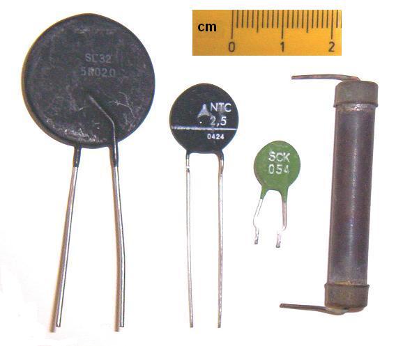